

1. Introduction to the principle of hash board:
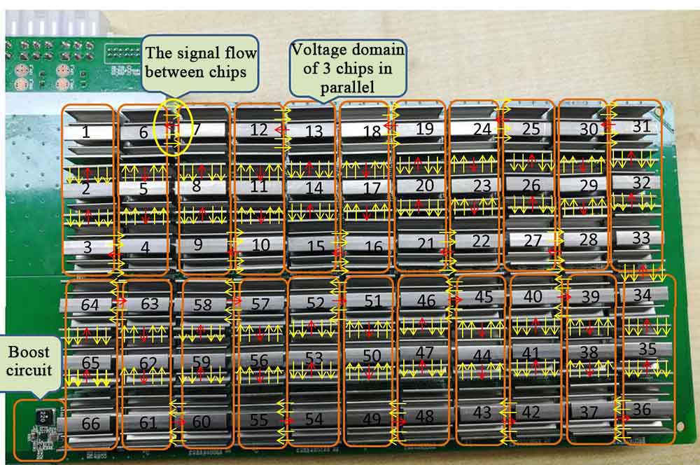
M1 is composed of 22 voltage domains in series, each voltage domain has 3 SMIT1700 chips in parallel, and there are 66 SMIT1700 chips on the whole board. Each voltage domain has an independent LDO to provide IO voltage and PLL voltage, the D05 version has an independent 24M clock circuit for each voltage domain, D06 is the clock provided by the previous chip, and each chip has an independent small heat sink on the front and back device, the front small heat sink (A) and the chip are fixed by a black glue with good thermosetting adhesive. The small heat sink (B) on the back is soldered to the chip's ground, so the heat sink B is charged and has voltage to the ground. Particular attention should be paid during maintenance to prevent short circuits.

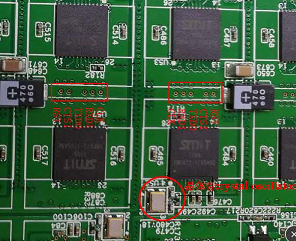
As shown in the figure above, there are 5 signals in the communication between chips. The arrow shows the signal flow. Each signal has test points on the front and back sides. They are arranged from left to right: CLK, RXDI, TXDO, CTS, RST or RST, CTS, TXDO, RXDI, CLK; the CLK test point is close to the crystal side.

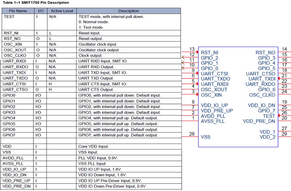
2. SMIT1700 chip pin definition:

3. Schematic diagram in a single voltage domain:

1) The clock circuit composed of crystals Y1 and U1 generates a clock and outputs it to the next chip through CLKO. V1.0 PCB D05 version has a crystal for each voltage domain; D06 is the last chip of each layer of voltage domain and is output to the next layer of voltage domain through level conversion;
2) U67 is an LDO, and the input voltage of the LDO comes from the fourth layer voltage domain behind the layer voltage domain, outputs 1.8V to the IO power supply, and generates a PLL voltage of about 0.9V through the resistance divider;
3) Diodes and pull-up and pull-down resistors form a level conversion circuit, which connects signals across different voltage domains.
4. Schematic diagram of the boost circuit:
The 12V is boosted to 16V through the TPS6116 to provide the input voltage for the LDO in the last 6-layer voltage domain.

5. Voltage domain filter capacitors for each layer:

6. Maintenance steps:

Observation of appearance: Observe whether there is displacement, deformation, and burning of small heat sinks? If there is, it must be dealt with first; observe whether there is burnout of the device, and clean up the burnt device first.
Measure impedance: Use the resistance gear of a Fluke 17B+ multimeter to measure whether there is a short circuit in the voltage domain of each layer. If the resistance value is below 2R or above 7R, it can be judged that there is abnormal chip resistance in the voltage domain of this layer. It shows parts in the abnormal voltage domain with open circuit and short circuit phenomena. The most likely cause is the general chip. But there are three chips in each voltage domain, and often only one of them fails when it fails. The method to find out the problem chip can be detected and compared to find the abnormal point through the test point-to-ground impedance of each chip. If you encounter a short circuit, you can remove the heat sink on the chip with the same voltage, then observe whether the chip pins are connected to tin. If there is no short-circuit point by appearance, you can find the short-circuit point according to the resistance or current cutoff method.
Measuring voltage: Use Fluke 17B+ multimeter to measure whether the voltage of each layer is between 0.5~0.7V.
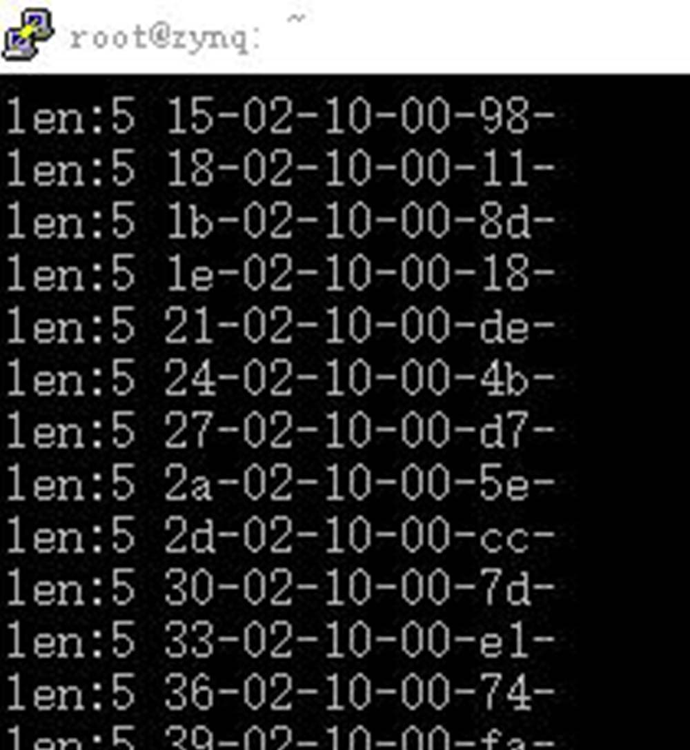
Use the test program to read the chip ID; as shown in the figure below, the communication cannot be performed; it can be judged that the TXDI PIN of pin 21 of the chip is not pulled high; you can measure the test point TXDO through a multimeter, and quickly locate a particular place where TXDO is not pulled up using half-folding search, and analyze whether the connected chip is damaged.

Use the test program to read the chip ID. If it is found that there are only three chips or less and the chip ID cannot be read, use an oscilloscope to check whether each chip has a clock input. Because there is no clock input, the test program will skip the chip. If it is found that part of the chip ID is read, it will be terminated. In addition to checking the clock, you must use an oscilloscope to check whether there are waveforms in TXDO and RXDI to determine whether the signal is normal and locate the position where there is no waveform. Check the level conversion circuit composed of diodes and pull-up resistors if it is a position across the voltage domain. If there is no problem, the adjacent chips at this position may be poorly soldered or damaged.
You can use the test program to run 10,000 times for waveform measurement.
./bitmicro-test /dev/ttyS2 1000000 10000 1 read_chip_model 66
