


Antminer S19 Hydro Hash Board Repair Guide
Ⅰ. Maintenance platform/tool/equipment preparation requirements
1. Platform requirements:
Static repair workbench (the workbench needs to be grounded), anti-static bracelet and grounding.
2. Equipment requirements:
Constant temperature soldering iron (350℃ to 380℃), pointed soldering iron tip is used to solder small patches such as SMD resistors and capacitors. A hot air BGA rework station is used for chip/BGA disassembly and soldering. Multimeter, attach a welded steel needle and cover it with a heat shrink sleeve for easy measurement (Fluke recommended). Oscilloscope (Agilent recommended), network cable (requirements: connected to the Internet, stable network).
3. Test tool requirements:
The APW9 / APW9+ / APW11 PSU is used to power the hash board ( DIY power adapter cable: use thick copper wires for the positive and negative poles of the power supply to connect the power supply and the hash board. It is recommended to use 4AWG copper wire with a length of less than 60cm). Test fixture using V2.2040 control board (test fixture material number ZJ0001000001)
4. Requirements for repair auxiliary materials / tools:
Solder paste M705, flux.
Washing water with anhydrous alcohol is used to clean the flux residue after repair.
Tin tools, tin removal tools, solder balls (recommended ball diameter is 0.4mm).
When replacing a new chip, the chip pins need to be tinned and then welded to the hash board. Apply thermal conductive silicone grease evenly on the surface of the chip and then lock the water-cooling heat sink.
5. Common repair spare material requirements:
0402 Resistor (0R, 10R, 33R, 100R, 1K, 2K), 0402 Capacitor (0.1uf, 1uf)
Ⅱ. Repair requirements
1. Pay attention to the operating techniques when replacing the chip. There is no obvious deformation of the PCB after replacing any accessories. Check the replacement parts and surrounding parts to see if there are any open or short-circuit problems.
2. Maintenance personnel must have certain electronic knowledge, more than one year of repair experience, and be proficient in BGA/QFN/LGA packaging welding technology.
3. After repair, the hash board must be tested more than twice and both are OK before it can pass!
4. Check whether the repair tools and test fixtures can work normally, and determine the repair station test software parameters, test fixture versions, etc.
5. When repairing or replacing a chip, you need to test the chip first and then do a functional test after passing it. Functional testing must ensure that the water-cooling plate is assembled properly. When installing the water-cooling plate, the surface of the chip must be evenly coated with thermal conductive gel. And the cooling fan is at full speed.
6. When measuring signals, 4 fans are assisted for heat dissipation and the fans maintain full speed.
7. When powering on the hash board, you must first connect the negative copper wire of the power supply. Before testing the pattern, the repaired hash board must cool down before testing, otherwise, it will cause test PNG.
8. When replacing a new chip, the pins and solder paste must be printed to ensure that the chip is pre-tinned and then soldered to the PCBA for repair.
9. The fixtures on the repair end all use the Test_Mode mode and are tested in the scan code mode. After the test pass, the production end is streamlined from the first test station, and the equipment is installed and aged normally (installed at the same level).
Ⅲ. Fixture production and precautions
The fixture set should satisfy the heat dissipation of the hash board and facilitate signal measurement.
1. Material number: ZJ0001000001 test fixture.
2. When using the S19 Hydro series test fixture for the first time, use the SD card flash program to update the FPGA on the fixture control board. After decompression, copy it to the SD card and insert the card into the jig card slot. Power on for about 1 minute and wait for the indicator light on the control board to double flash three times before the update is completed (if it is not updated, a certain chip may be reported as defective during the test).

Figure 3-1
3. Make the test SD card according to the requirements. PT1 chip detection, PT1+ chip detection +50M, PT2 function test, directly unzip the compressed package to create an SD card. After unzipping, delete the original Config file first, then Config.ini-HHB28601-PT2 configuration file and rename it to Config.ini. Then click "Yes" and the final configuration file is "Config".
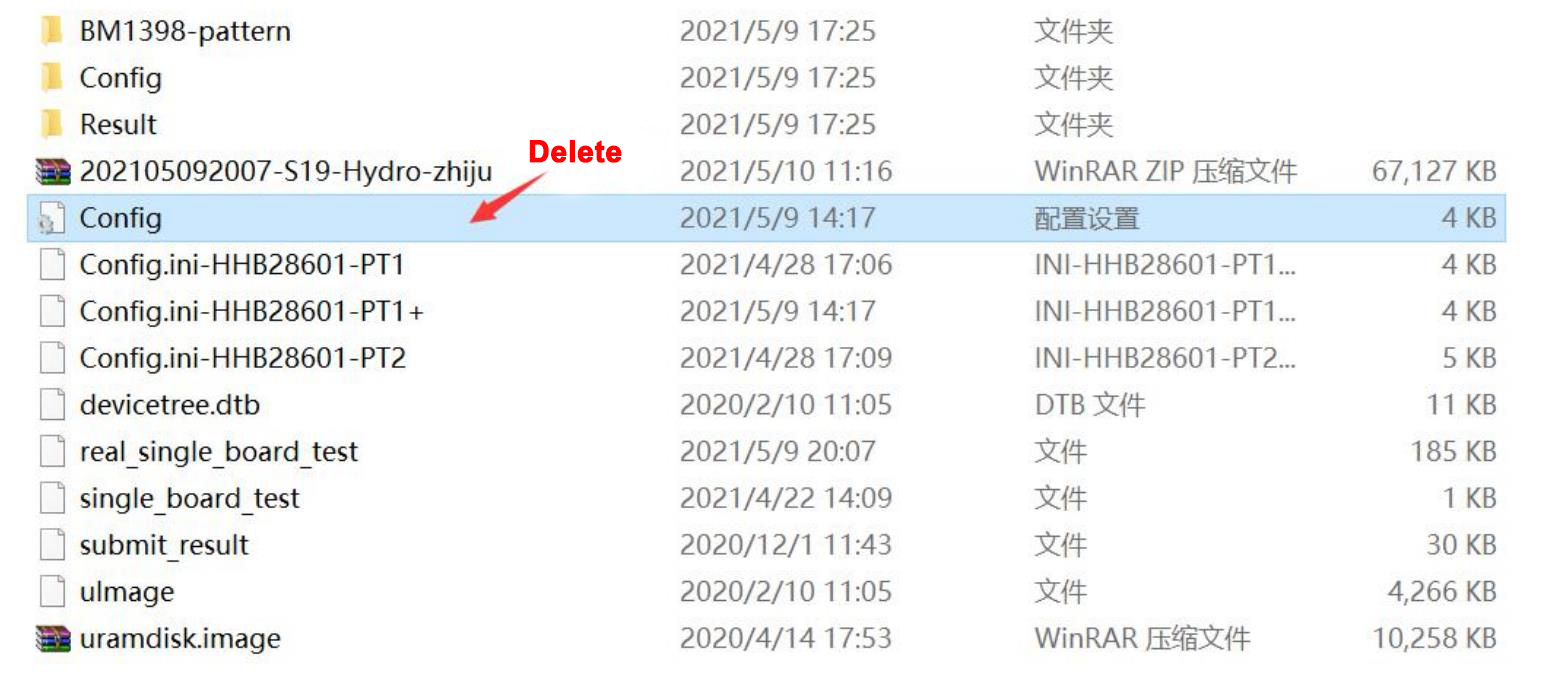
Figure 3-2
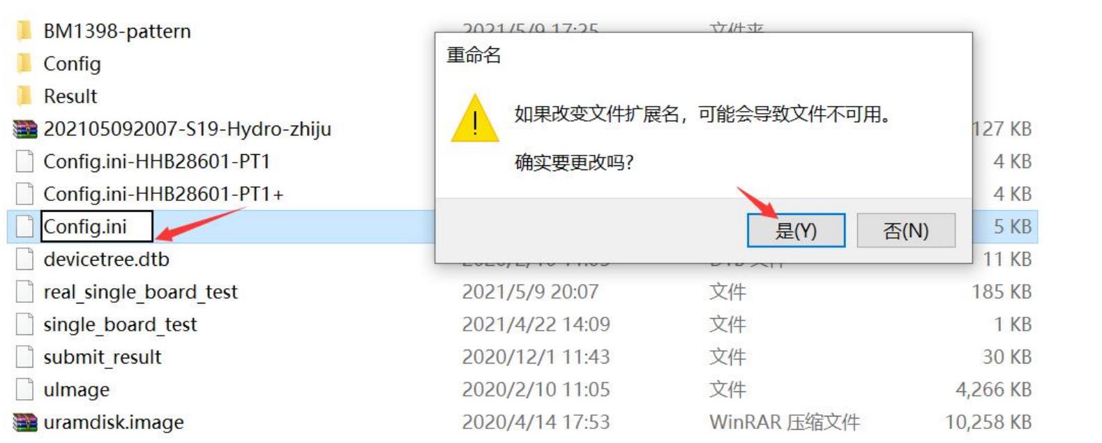
Figure 3-3
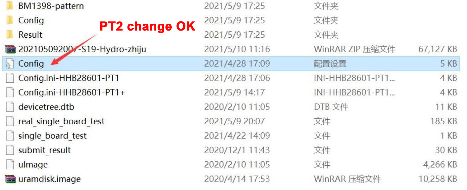
Figure 3-4
4. The S19 Hydro test cable requires manual modification. One end of the modified test cable is connected to the power adapter board, and the other end of the unmodified test cable must be connected to the test fixture. Note that if the test cable is connected incorrectly or the test fixture is connected incorrectly, PIC FAIL will be reported.
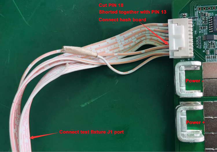
Figure 3-5
Ⅳ. Principle Overview
1. S19 Hydro hash board working structure:
The hash board consists of 104 BM1398 chips (silk screen sequence BM1-BM104) divided into 52 groups (domains), each group consisting of 2 ICs. The BM1398 chip used in the S19 Hydro hash board operates at 0.37V. Groups 52, 51, 50, 49, 48, 47, and 46 (7 groups in total), the 25V output by the boost circuit U9 supplies power to the LDO and outputs 1.8V. Group 45 to Group 1 are provided 1.8V by VDD 18V through LDO. Each time one domain is moved back, the domain voltage decreases by 0.37V. All 0.8V is provided by the 1.8V of this domain through the LDO output, as shown in Figure 4-1:

Figure 4-1
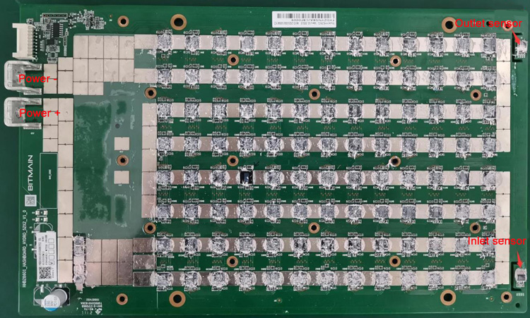
Figure 4-2
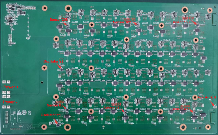
Figure 4-3
2. S19 Hydro hash board boost circuit:
The boost circuit converts the power from 19V to 25V, as shown in Figure 4-4.
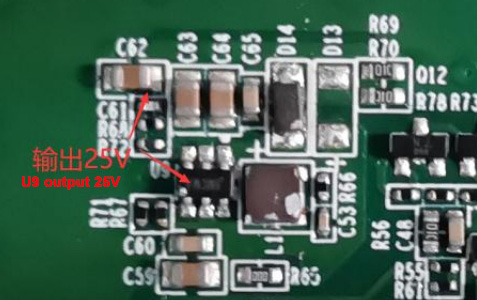
Figure 4-4
3. S19 Hydro chip signal direction:
CLK signal flow direction: generated by Y1 and Y2 crystal oscillator 25M. Y1 is transmitted from BM1 chip to BM51 chip. Y2 is transmitted from the BM52 chip to the BM104 chip, and the voltage is about 0.9V.
TX (CI, CO) signal flow direction: from the 7th pin (3.3V) of the IO interface to the level conversion IC U2, and then transmitted from the BM1 chip to the BM104 chip. When the IO cable is not plugged in, the voltage in standby is 1.8V and the voltage in operation is 0.6V.
RX (RI, RO) signal flow direction: from BM104 chip to BM1 chip, back to pin 8 of the signal cable terminal via U1, and then back to the control board. The voltage is 0.3V when the IO cable is not plugged in, and the voltage is 1.8V during operation.
BO (BI, BO) signal flow direction: from BM1 chip to BM104 chip, measured by multimeter is 0V.
RST signal flow direction: from the 3rd pin of the IO interface to D2, R13, R14, and then transmitted from chip 01 to chip 104. When the IO cable is not plugged in, it is 0V in standby and 1.8V during operation.
4. Overall miner structure:
The miner mainly consists of 4 hash boards, 1 control board, and an APW11 power supply, as shown in Figure 4-5.
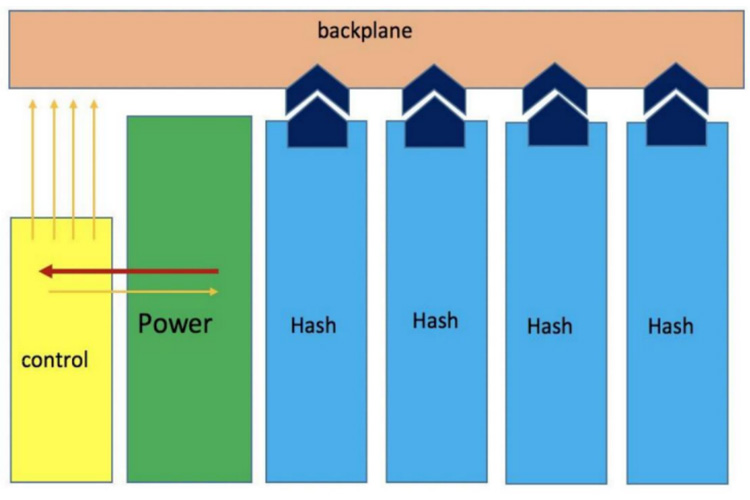
Ⅴ. Common adverse phenomena of hash boards and troubleshooting
1. Phenomenon: The single board test detection chip is 0 (PT1 station)
Step 1: Check the power output first, please check Figure 5-1.
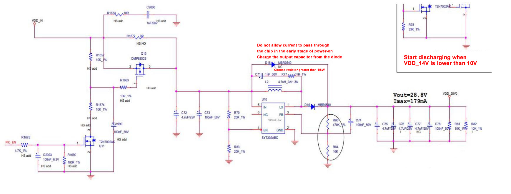
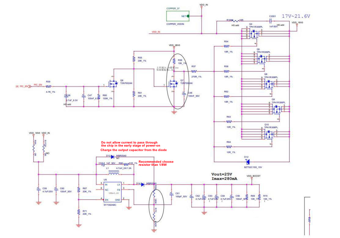
Figure 5-1
Step 2: Check the voltage output of the voltage domain.
The voltage of each voltage domain is about 0.37V. When the power supply is 19V, there is usually a domain voltage. Prioritize measuring the power terminal output of the hash board to check if the MOS is short-circuited (measure the resistance between pins 1, 4, and 8). If there is a 19V power but no domain voltage, continue troubleshooting.
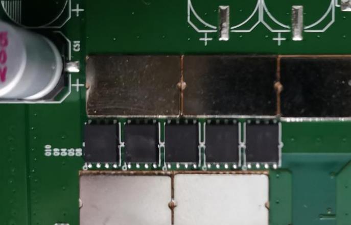
Figure 5-2
Step 3: Check the PIC circuit.
Measure whether there is output at pin 2 of U3, the voltage is about 3.2V. If so, please continue to troubleshoot the problem. If there is no 3.3V, please check the connection status of the fixture cable and the hash board. If it is OK, reprogram the PIC.
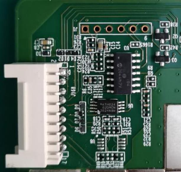
Figure 5-3
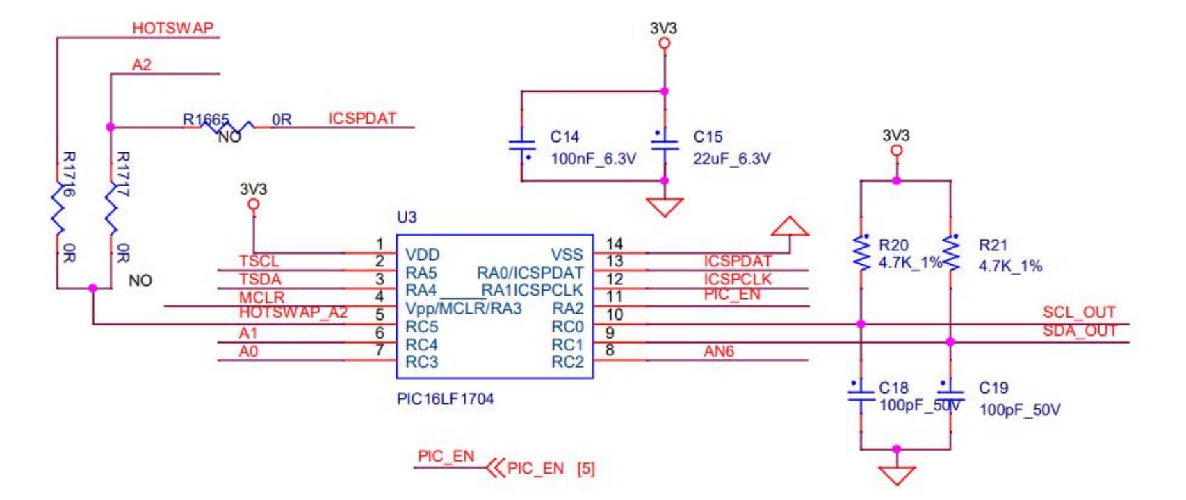
Figure 5-4
PIC programming procedures:
1). Burning the hash board PIC program.
Program: PIC_H20_release_v101_4c54.hex
Download programming tool: PICkit3. Pin 1 of the PICkit3 cable corresponds to pin 1 of J2 on the PCB board, pin 1, 2, 3, 4, 5, and 6 need to be connected.
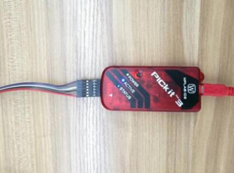
Figure 5-5
2). Burning software:
Open MPLAB IPE and select device: PIC16F1704. Click "power" to select the power method, then click "operate".
Step ①: Select “file” to find .HEX file to be burned.
Step ②: Click "connect" and the connection is normal.
Step ③: Click the "program" button, and click "verify" after completion. It will prompt that the verification is completed to prove that the burning is successful.

Figure 5-6
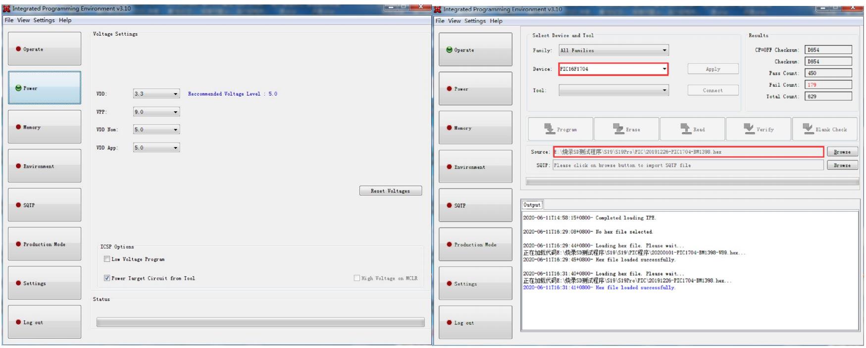
Figure 5-7
Step 4: Check the boost circuit output. In Figure 5-8, C76 can measure 28V voltage, and C62 can measure 25V voltage.
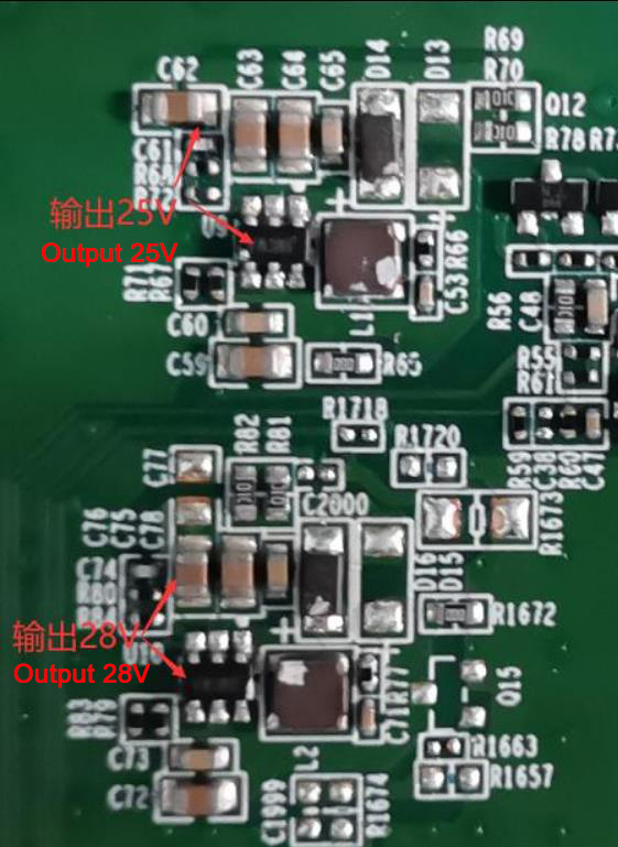
Figure 5-8
Step 5: Check each group of LDO 1.8V or PLL 0.8V output.

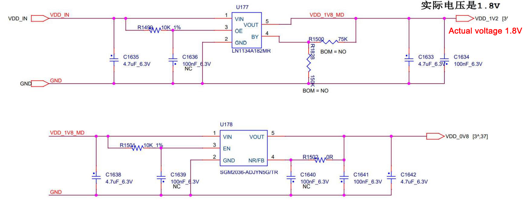
Figure 5-9

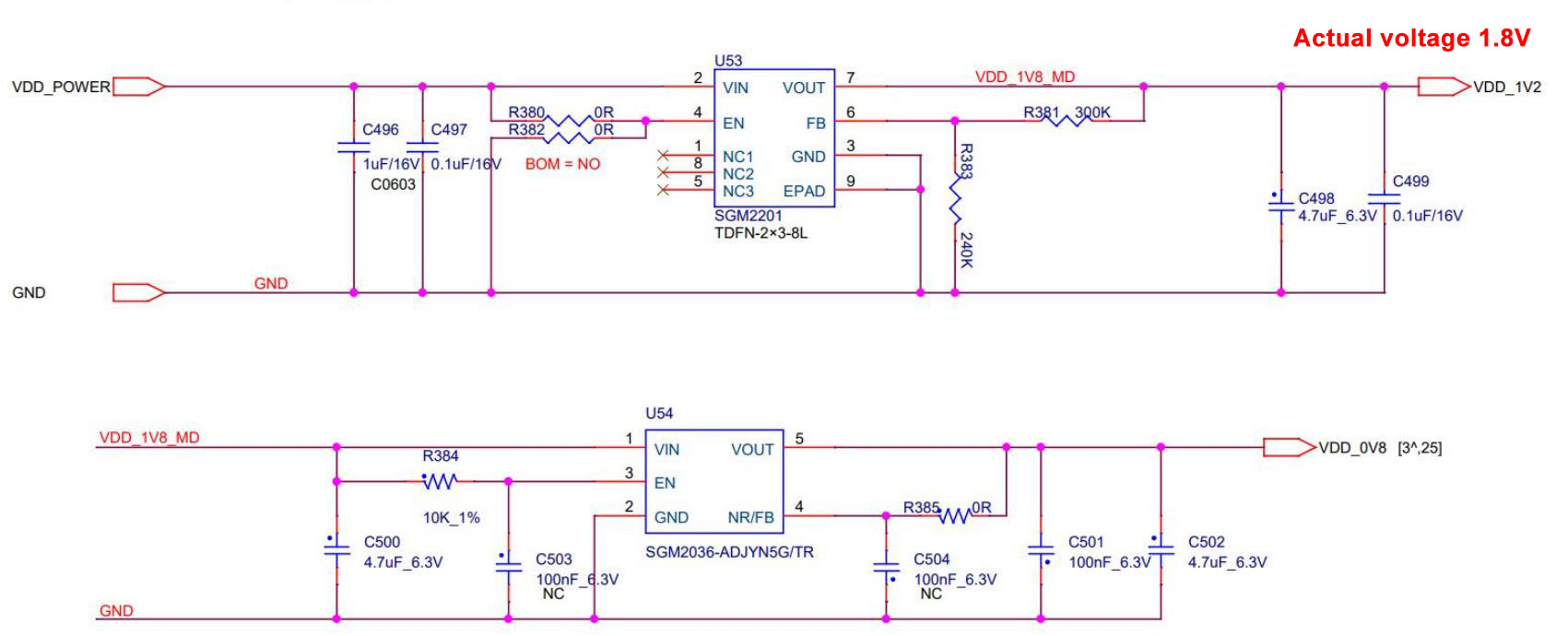
Figure 5-10
Step 6: Check the chip signal output (CLK/CI/RI/BO/RST).
The voltage value range described by the reference signal direction. If the measured voltage value deviates greatly from the reference value, it can be compared with the adjacent group of measured values.

Figure 5-11
2. Phenomenon: EEPROM NG is displayed on the LCD screen of the test fixture.
Check whether U6 is welded properly.
3. Phenomenon: When ASIC INIT NG is displayed on the LCD screen of the test fixture, the test reading temperature is abnormal.
Follow these steps to troubleshoot:
A) Check the serial port log. For example, when sensor=0, check whether the U251, U263, BM1 chips or the nearby chip resistors and capacitors are welded normally.
B) Sensor={0, 24, 48, 158, 182, 206} corresponds to the chip positions {BM1, BM13, BM25, BM80, BM92, BM104}.

Figure 5-12
4. Phenomenon: INIT NG WATER_TEMP is displayed on the LCD screen of the test fixture.
Test and read the abnormal temperature of the water inlet and outlet, and check whether U4, U5 and SMD resistors and capacitors are welded normally.
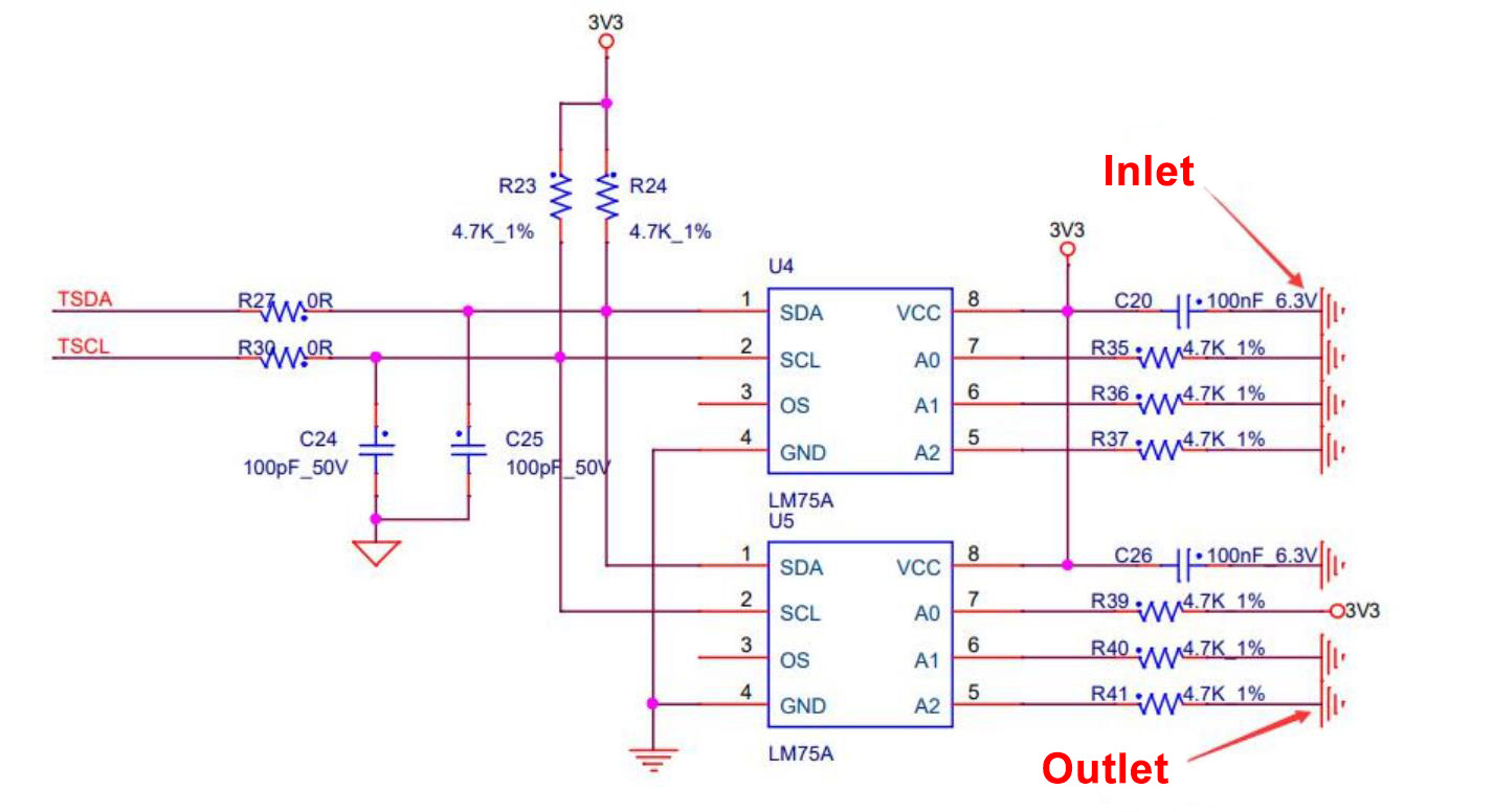
Figure 5-13
5. Phenomenon: The hash board indicator light does not light up.
Check if PIC 3.3V is normal.
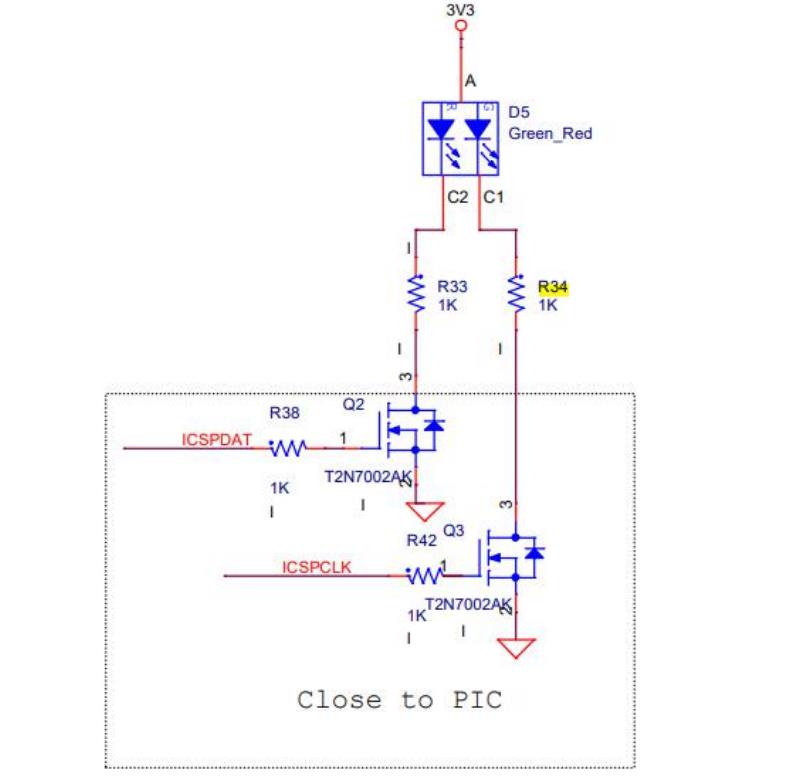
Figure 5-14
6. Phenomenon: The number of single board detection chips is incomplete (PT1/PT2 station)
a) When the LCD screen of the test fixture displays ASIC NG: (0). First, measure the total domain voltage of 21V and the boost circuit voltage of 25V to see if they are normal. Then use the multimeter short-circuit probe to short-circuit the RO test point and 1V8 test point between chip 1 and chip 2, and then run the chip finder program and look at the serial port log. If 0 chips are still found, then it will be one of the following situations:
a-1) Use a multimeter to measure whether the voltages at the 1V8 and 0V8 test points are 1.8V and 0.8V. If not, it may be that the 1.8V and 0.8V LDO circuits in this domain are abnormal, or the 2 ASIC chips in this domain are not soldered properly. Most of them are caused by the short circuit of the 0.8V and 1.8V patch filter capacitors (Measure the resistance value of the chip filter capacitor related to the front and back sides of the PCBA).
a-2) Check whether the U1 and U2 circuits are abnormal. Such as resistor virtual soldering, etc.
a-3) If 1V8 and 0V8 are normal, measure RO, RST, CLK, CI, and BI signals in sequence to see if they are normal.
a-4) Abnormal water temperature or abnormal heat dissipation causes U4 and U5 to burn out. PIC chip U3 is short-circuited to ground, the 1.8V and 0.8V of the first domain have no output, and the BM1 and BM2 chips are burned out. (U4, U5, U1, U2, U177, U178, BM1, BM2 are burned out)
b) If one chip can be found in step a), it means that the 1st chip and the previous circuit are normal. Use similar method to troubleshoot the subsequent chips.
For example, if the 1V8 test point and RO test point between the 38th and 39th chips are short-circuited, if the log can find the 38th chip, then there is no problem with the previous 38 chips. If 0 chips are still found, first check whether the 1V8 is normal. If 1V8 is normal, there is a problem after chip 38. Continue using the dichotomy method until you find the problematic chip. Assuming that there is a problem with the Nth chip, then when 1V8 and RO between the N-1th and Nth chips are short-circuited, the N-1 chip can be found. But when 1V8 and RO between the N and N+1 chips are short-circuited, the total number of chips cannot be found.
c) The LCD screen of the test fixture displays ASIC NG: (X). When a certain chip is fixedly reported, there are two situations:
c-1) Case 1: The test time is basically the same as that of the OK board, and usually the value of X does not change each time it is tested. (The test time refers to the time from pressing the start test button to the LCD displaying the result ASIC NG: X). This situation is most likely caused by abnormal welding of the upper and lower CLK, CI, and BO resistors of the X chip, so just focus on checking these 6 resistors. A few cases are caused by abnormal welding of the following pins of the three chips X-1, X, and X+1.
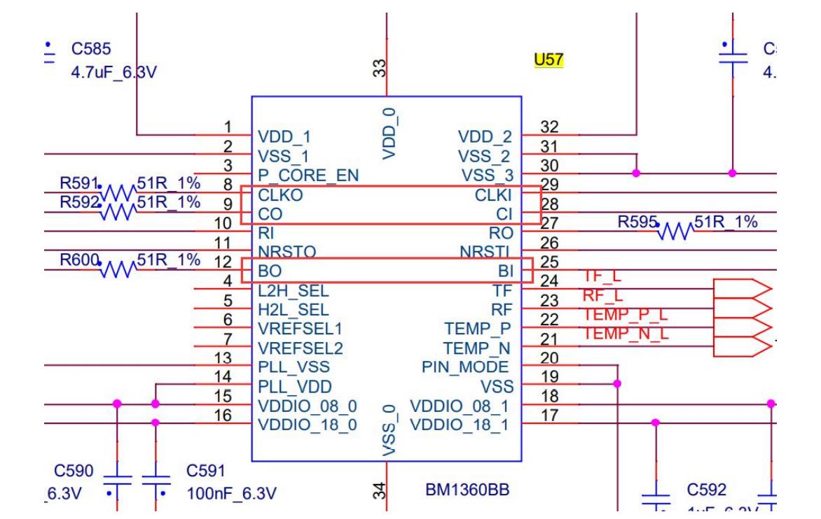
Figure 5-16
c-2) The second case: the test time is almost twice as long as that of the OK board (Sometimes the X value changes each time the test is performed, and sometimes X=0).
During testing, it is assumed that the domain voltages of all domains before the abnormal position are almost all less than 0.3V and that the domain voltages of the domains after them are almost all higher than 0.37V. This situation is caused by the chip not being soldered properly, usually 1.8V, 0.8V, RXT, CLK are not soldered properly. It is recommended to directly measure the domain voltage to locate the location of the faulty domain. The 1V8 and RO short circuit method used in section a) can also locate the abnormal location.
c-3) The third situation: There is no abnormality in the appearance of the chip and the voltage signal is normal. It is a problem with the chip itself.
7. Phenomenon: The single board Pattern NG, that is, the reply nonce data is incomplete (PT2 station).
Pattern NG is caused by the characteristics of certain chips being quite different from other chips. There are currently several adverse causes:
1) If the chip die is found to be damaged, only need to replace the chip.
2) Chip tin bridge, chip virtual soldering (the noce reply number of two chips in one domain is 0 or 1).
3) The domain voltage of this domain is low, the 1.8V and 0.8V voltage is normal, and it is a problem with the chip itself.
4) The number of noce replies for multiple chips is 0. Measure the domain voltage and start troubleshooting the domain from lower domain voltage.

Figure 5-17
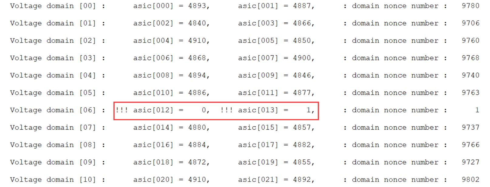
Figure 5-18
Please note that the numbers of domain and asic both start from 0.
8. Phenomenon: chip detection test is OK, PT2 function test serial port does not stop (long time running)
Repair method: During the PT2 test, check the serial port print log. It is usually caused by an error in the register address of a certain chip. Just replace the BM5 chip as shown in Figure 5-19 (ASIC starts from 0).
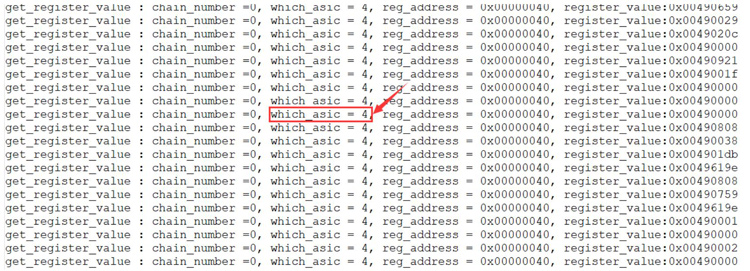
Figure 5-19
9. Phenomenon: The PT1 chip test is OK, and the PT2 function test always reports a certain chip NG.
Repair method: Check the appearance and measure the chip capacitance or resistance on the front. Generally, it is caused by poor chip welding or damage and abnormal resistance of a certain chip capacitor or resistor, or a problem with the chip itself.
Ⅵ. Problems caused by control board failure
1. The whole machine is not running
1) Check whether the voltage at voltage output points is normal. If 3.3V is short-circuited, you can disconnect U8 first. If it is still short-circuited, you can unplug the CPU and measure. For other voltage abnormalities, generally replace the corresponding voltage converter IC.
2) If the voltage is normal, please check the welding status of the DDR/CPU.
3) Try updating the flash program using the SD card.
If the miner with the control board card flash needs to start normally, two steps are required:
a) After the card flash is successful, the green LED indicator light is always on, and then the power is turned off and restarted;
b) Wait 30 seconds after powering on again (the time required to turn on OTP).
OTP (One Time Programable) is a memory type of MCU, which means one-time programmable: after the program is burned into the IC, it cannot be changed or cleared again.
Things to note:
(1) A sudden power outage or less than 30 seconds during the process of opening OTP will cause the control board to fail to open the OTP function and the control board will not start (not connect to the Internet). U1 (control board main control IC FBGA) needs to be replaced. The replaced U1 cannot be used on the 19 series.
(2) For control boards with the OTP function enabled, U1 cannot be used on other series of models.

Figure 6-1
2. The miner cannot find the IP
There is a high probability that the IP cannot be found due to abnormal operation. Please refer to point 1 for troubleshooting.
Check the appearance and welding condition of the network port, network transformer T1, and CPU.
3. The miner cannot be upgraded
Check the appearance and welding condition of the network port, network transformer T1, and CPU.
4. The miner fails to read the hash board or miss chain, reporting J:4.
A. Check the cable connection status.
B. Check the parts of the control board corresponding to the chain.
C. Check the wave soldering quality of the pins and the resistance around the plug-in interface.
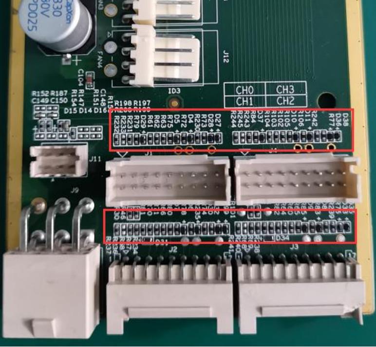
Figure 6-2
Ⅶ. Whole machine failure phenomenon
1. Initial test of the whole machine
Referring to the test process document, the general problems are assembly process problems and control board process problems.
Common phenomena: IP cannot be detected, abnormal number of fans detected, abnormal chain detection. If an abnormality occurs during the test, repairs must be carried out according to the monitoring interface and test LOG prompts. The repair methods for the initial test of the whole machine and the aging test are the same.
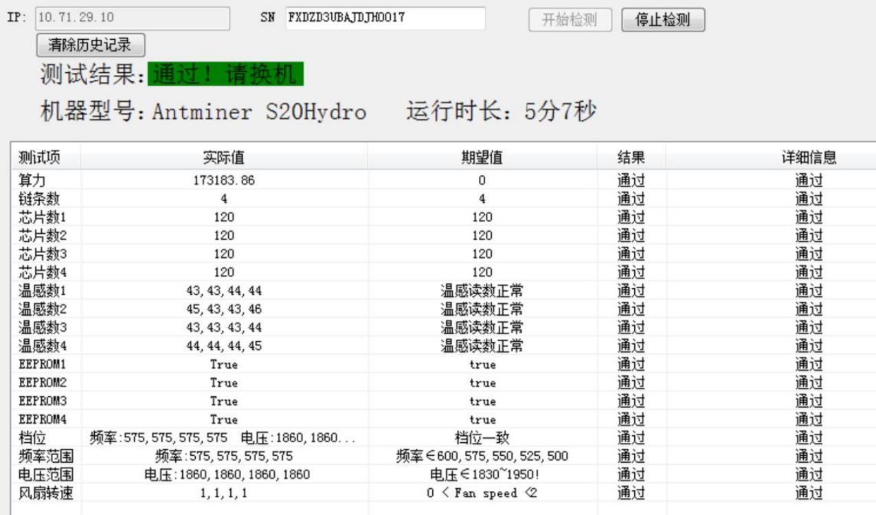
Figure 7-1
2. Aging test: During the aging test, repair must be carried out according to the monitored interface test.
1) The fan display is abnormal: Check whether the fan is working normally, whether the connection with the control board is normal, and whether there is any abnormality in the control board.
2) Missing chain: Missing chain means 1 piece is missing from 3 hashboards. In most cases, there is a problem with the connection between the hash board and the control board. Check the cable to see if there is an open circuit. If the connection is OK, you can Perform the PT2 test on the single board to see if it can pass the test. If it can pass the test, it can basically be determined that it is the control board. If it cannot pass the test, use the maintenance method to repair PT2.
3) Abnormal temperature: Generally, it is caused by high temperature. The maximum temperature of the machine set by the monitoring system cannot exceed 103 degrees. If it exceeds 103 degrees, the machine will alarm and cannot work normally. This is usually caused by excessive ambient temperature and abnormal working of the fan causing temperature abnormalities.
4) Not all chips can be found (it can still be turned on, but the hash rate is 2/3 or 1/3 of the normal value), that is, the number of chips is not enough: If the number of chips is not enough, you can refer to the PT2 test for repair.
5) No hash rate after running for a while. The mining pool connection is interrupted, check the network.
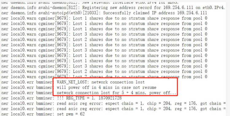
Figure 7-2
3. After-sales repair, production repair water-cooling test platform construction
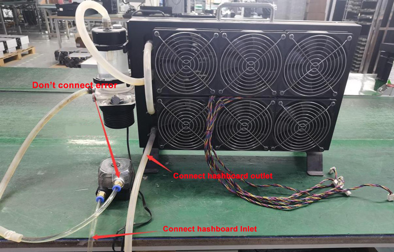
Figure 7-3
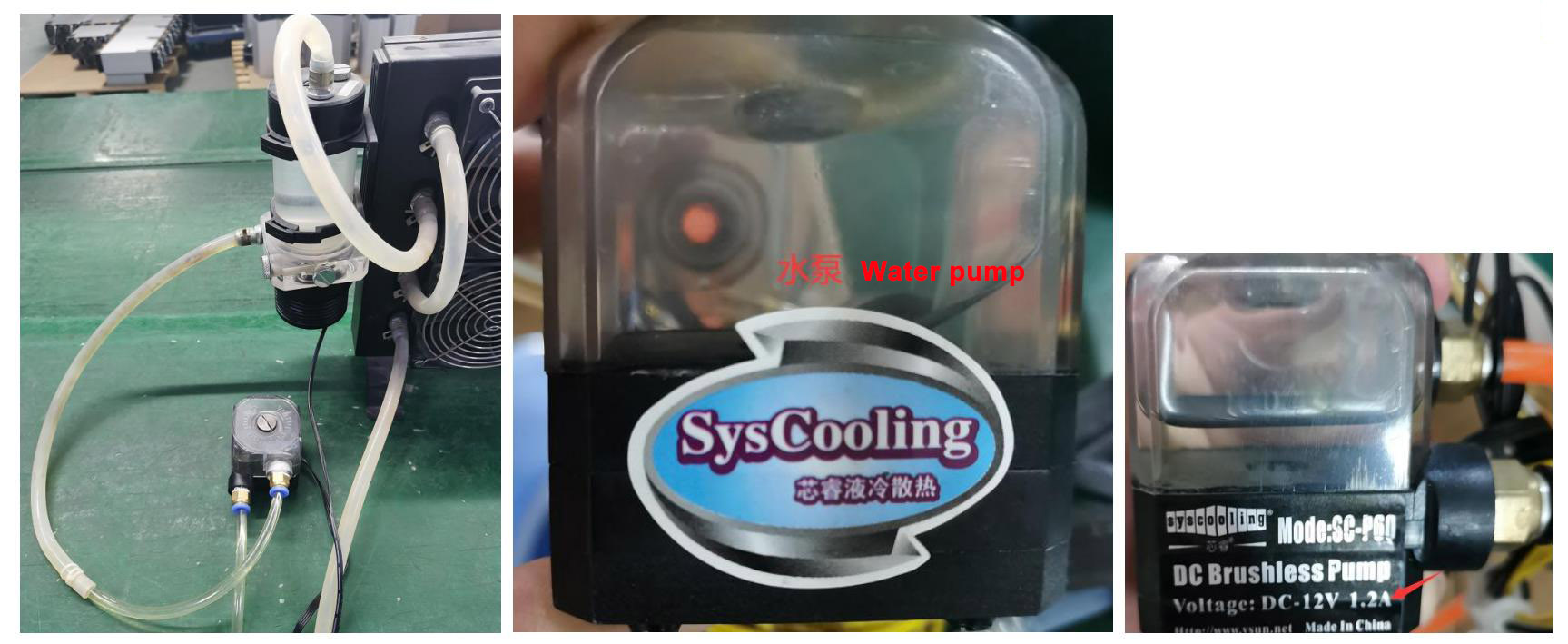
Figure 7-4
1) Because the first-generation water-cooled radiator cannot meet the heat dissipation requirements, it is necessary to add a water pump in series (or two water radiators in series) during the transformation;
2) Use 8mm air pipe connectors and air pipes when retrofitting;
3) If the heat dissipation cannot meet the requirements, an air-cooling fan can be added to assist;
Refer to the above troubleshooting steps for each station. Please communicate with the after-sales engineer for the relevant test procedures and test fixture usage details. After repair, you can use the scan code mode to test PT2.
Ⅷ. Other notes
Repair flow chart

Figure 8-1 Repair flow chart
Routine detection: First, conduct a visual inspection of the hash board to be repaired to see if there is PCB deformation or scorching. If any, it must be dealt with first. Are there any parts with obvious burn marks, parts that are offset due to impact or missing parts, etc. Secondly, if there is no problem after visual inspection, you can first test the impedance of each voltage domain to detect whether there is a short circuit or open circuit. If found, it must be dealt with first. Finally, check whether the voltage of each domain is about 0.37V.
After there is no problem in the routine inspection (short circuit detection of the general routine inspection is necessary to avoid burning the chip or other materials due to short circuit when the power is turned on). The test fixture can be used for chip detection, and the positioning can be determined based on the test results of the test fixture.
According to the display results of the test fixture detection, start from the vicinity of the faulty chip and detect the chip test points (CI/RST/RO/CLK/BI) and VDD0V8, VDD1V8 and other voltages.
According to the signal flow direction, except for the RO signal which is transmitted in the reverse direction (from chip 104 to chip 1), several other signals CLK CI BI RST are transmitted in the forward direction (from chip 1 to chip 104). The abnormal fault point is found through the power supply sequence.
When locating the faulty chip, the chip needs to be re-soldered. The method is to add flux around the chip, preferably no-clean flux. Heating the solder joints of the chip pins until they are in a dissolved state will prompt the chip pins and pads to re-break in and collect the tin to achieve the re-tinning effect. If the fault remains the same after re-soldering, the chip can be replaced directly.
After the repair, the hash board must be passed twice or more before it can be judged to be qualified when tested by the test fixture. For the first time, after replacing the accessories, wait for the hash board to cool down, use the test fixture to test the pass, and then set it aside to cool down. The second time, wait a few minutes for the hash board to cool completely before testing again.
After the hash board is repaired, relevant maintenance/analysis records need to be made (repair report requirements: date, SN, PCB version, tag number, cause of failure, attribution of responsibility for failure, etc.). In order to provide feedback to production, after-sales, and R&D.
For repaired hash boards, the thermal grease must be removed and reprinted water-cooling board.
After recording, install the complete machine for routine aging.
We use cookles to Improve your online experience. By continuing browsing this website, we assume you agree our use of cookies.