


Antminer S19j Pro+ BHB42611 Hash Board Repair Guide
Ⅰ. Maintenance platform/tool/equipment preparation requirements
1. Platform requirements:
Static repair workbench (the workbench needs to be grounded), anti-static bracelet and grounding.
2. Equipment requirements:
Constant temperature soldering iron (350 degrees-380 degrees), pointed soldering iron tip is used to solder small patches such as chip resistors and capacitors. A hot air gun, heating station (350℃-400℃), and BGA rework station are used for chip / BGA disassembly and soldering. Multimeter, add welded steel pins and put on heat shrink tube for easy measurement (Fluke is recommended). Oscilloscope, network cable (requirements: connected to the Internet, stable network).
3. Test tool requirements:
APW12 PSU (the machine itself uses the power supply), DIY power adapter cable: The positive and negative poles of the PSU use thick copper wires to connect the power supply and the computing board. It is recommended to use 4AWG copper wire with a length within 60cm, limited to PT1 and maintenance testing, for hash board power. Use the test fixture of V2.1 or V2.3 control board (test fixture part number ZJ0001000001). The positive and negative poles of the power supply of the test fixture need to be equipped with discharge resistors. It is recommended to use cement resistors of 20 ohm and above 100W.
4. Requirements for repair auxiliary materials/tools:
Solder paste M705, flux, board washing water with anhydrous alcohol (board washing water is used to clean up the flux residue after repair). Thermal grease (used to apply on the chip surface after repair). Tin-planted steel mesh (6mm * 6mm chip size), desoldering wire, Tin ball (ball diameter recommended: 0.4mm). When replacing a new chip, need to tin the chip pins and then solder them to the hash board. Apply thermal conductive silicone grease evenly on the chip surface and then lock the water-cooling heat sink.
5. Common repair spare material requirements:
0402 resistor (0R, 33R, 51R, 10K, 4.7K), 0402 capacitor (0.1uf, 1uf).
Ⅱ. Repair requirements
1. Pay attention to the working method when replacing the chip. There will be no obvious deformation of the PCB board after replacing any accessories. Check whether there are open or short circuit problems in the replacement parts and surrounding parts.
2. Maintenance personnel must have certain electronic knowledge, more than one year of repair experience, and be proficient in BGA/QFN/LGA packaging welding technology.
3. After repair, the hash board must be tested more than twice and both are OK before it can pass!
4. Check whether the repair tools and test fixtures can work normally, and determine the repair station test software parameters, test fixture versions, etc.
5. For testing after repairing and replacing the chip, you need to pass the PT1 detection chip first, and then do the functional test. Functional testing must ensure that the small-sized heat sink is welded OK and the large-sized heat sink is installed in place (be sure to install the large heat sink after evenly applying thermal conductive silicone grease), and the cooling fan is at full speed. To use chassis cooling, 2 hash boards must be placed at the same time to form an air duct.
6. When measuring signals, 4 fans are assisted for heat dissipation and the fans maintain full speed.
7. When powering on the hash board, you must first connect the negative copper wire of the power supply, then connect the positive copper wire of the power supply, and finally plug in the signal cable. The order of disassembly must be reversed from the order of installation. Remove the signal cable first, then the positive copper wire of the power supply, and finally the negative copper wire of the power supply. If do not follow this order, it is very easy to cause damage to U1 and U2 (not all chips can be found). Before testing the pattern, the repaired hash board must be cooled down before testing, otherwise, it will cause the test PNG.
8. When replacing a new chip, the pins and solder paste must be printed to ensure that the chip is pre-tinned and then soldered to the PCBA for repair.
9. The chip of the BHB42611 model is a BSM process, that is, the surface of the chip uses a copper plating process. The heat sink is soldered directly to the chip with tin. During repair, it is required to remove the heat sink above the chip first. The temperature of the hot air gun is adjusted to 400°C. The air gun nozzle is 0.5CM above the heat sink. The heating time is 15 seconds and the heat sink can be removed. Then use the same temperature and method to blow the heat sink on the back of the chip, and use the same temperature and time to remove the heat sink on the PCBA on the back of the chip. Finally, weld the chip using conventional methods.
Ⅲ. Fixture production and precautions
The fixture set should satisfy the heat dissipation of the hash board and facilitate signal measurement.
1. Material number: ZJ0001000001 test fixture.
2. When using the 19 series test fixture for the first time, use the SD card flash program to update the FPGA on the fixture control board. After decompression, copy it to the SD card and insert the card into the fixture card slot. Power on for about 1 minute and wait for the indicator light on the control board to double flash three times before the update is completed (if it is not updated, a certain chip may be reported as defective during the test).

Figure 3-1
3. SD card production without heat sink: Repair uses the scan code PT1 program, as shown in the screenshot below, this program can be tested without scan code. The repair technician needs to dissipate heat from the PCBA when measuring to prevent the board from overheating during testing and measurement.
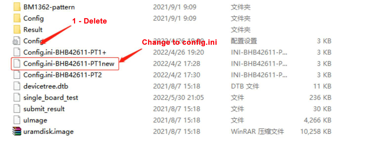
Figure 3-2
4. SD card production without heat sink: The double-sided heat sink 8x Patter test requires the production of an SD card, as shown in the figure below. Change the congfig.ini-BBK10601-PT2 file name to config.ini. There is no need to plug in the code scanner when testing PT2, just plug in the network cable. Please refer to the production heat dissipation method for the heat dissipation method (elements: insert the board into the chassis and lock the screws, power the board, the fans must be at full speed and the ambient temperature is less than 30°C).
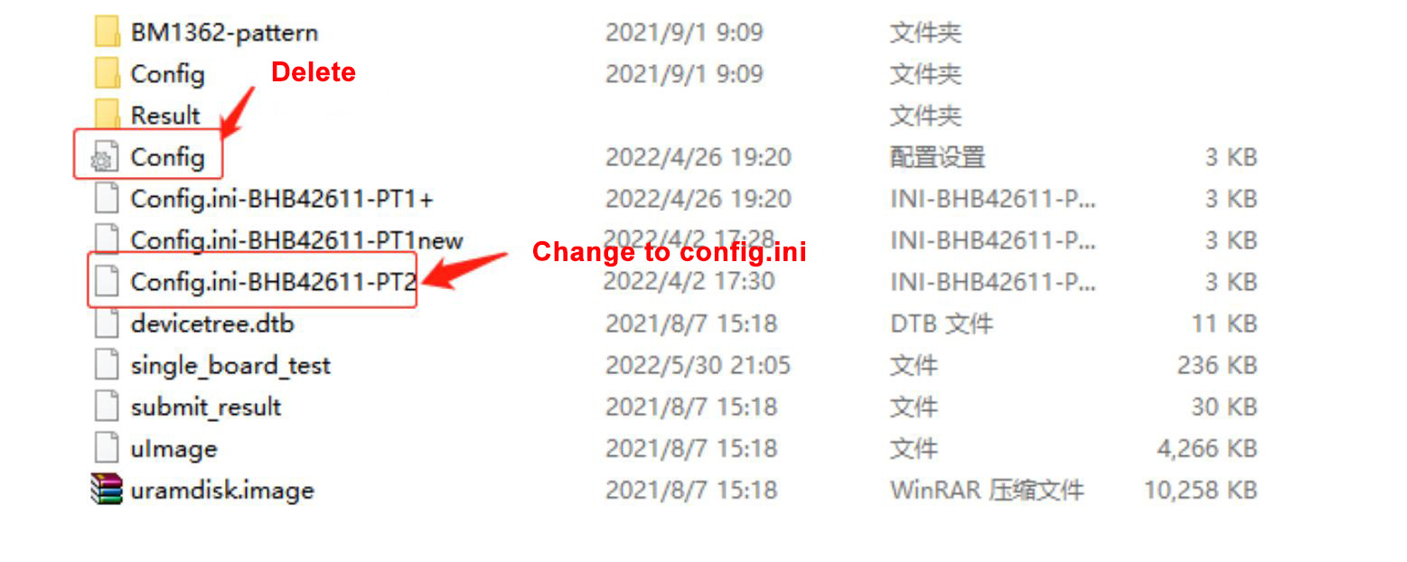
Figure 3-3
Ⅳ. Principle Overview
1. BHB42611 hash board working structure:
The hash board consists of 120 BM1362 chips divided into 40 groups (domains), each group consisting of 3 ICs. The BM1362 chip used in the BHB42611 hash board operates at 0.3V. The 40th, 39th, 38th, 37th, 36th, 35th and 34th groups (7 groups in total) are powered by the 19V output by the boost circuit U283 to the LDO. Make the LDOs of these 4 domains output 1.2V and 0.8V. The power supply of the remaining domain LDOs is VDD15V input and output 1.2V and 0.8V.
(PT2 test, computer log page starts counting from asic0, refer to Figure 4-1)
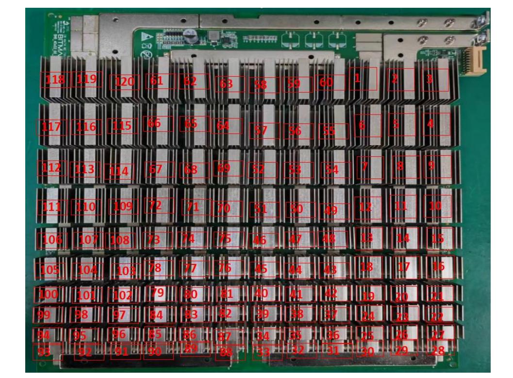
Figure 4-1
(The voltage domain in the test log starts from 0, that is domain0, refer to Figure 4-2)
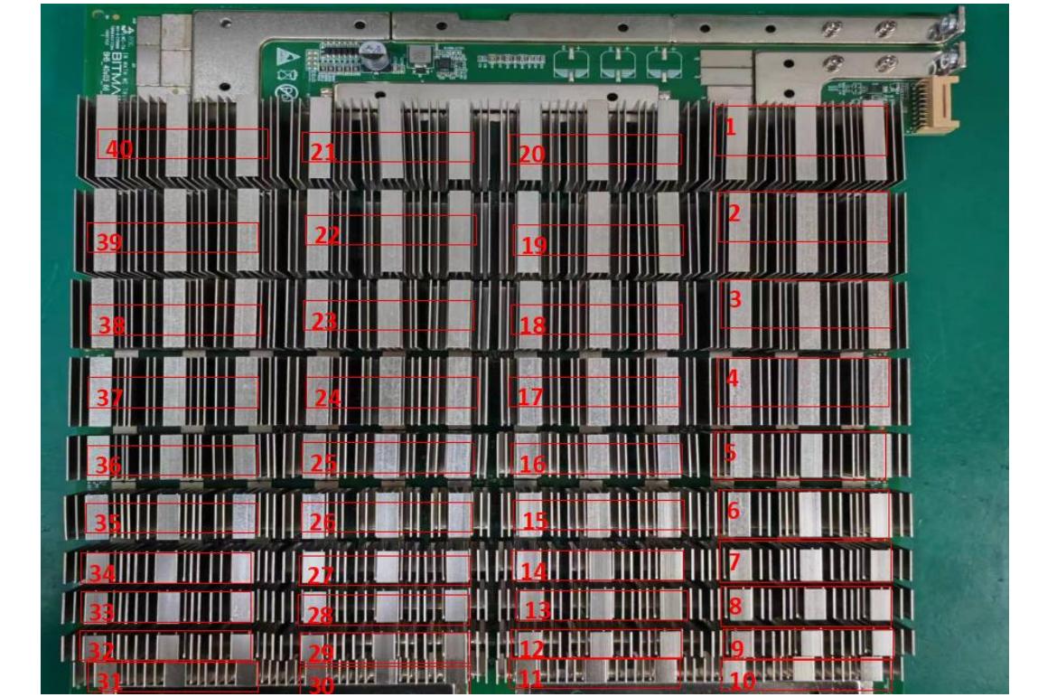
Figure 4-2
2. BHB42611 hash board boost circuit:
Boost circuit converts the power supply from 15V to 19V, as shown in Figures 4-3 and 4-4.

Figures 4-3

Figures 4-4
3. BHB42611 chip signal direction:
1) CLK (XIN) signal flow direction: generated by Y1 25M crystal oscillator, transmitted from chip 01 to chip 120.
2) RST signal flow direction: from pin 3 of the IO interface, and then transmitted from chip 01 to chip 120.
3) CI signal flow direction: from pin 7 of the IO interface, and then transmitted from chip 01 to chip 120.
4) RX (RI, RX) signal flow direction: from chip 120 to chip 01.
5) BO (BI, BO) signal flow direction: from chip 01 to chip 120.
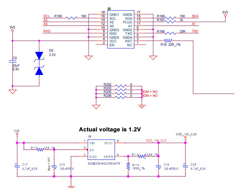
Figure 4-5
4. Whole machine structure:
The whole machine mainly consists of 3 hash boards, 1 control board, APW121417b power supply, and 4 cooling fans, as shown in Figure 4-6.
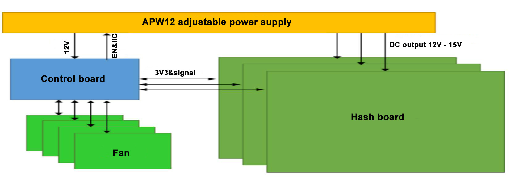
Figure 4-6
Ⅴ. Common adverse phenomena and troubleshooting of hash boards
1. Phenomenon: The single board test detection chip is 0 (PT1/PT2 station)
Step 1: Check the power output first.
Step 2: Check the voltage domain voltage output.
If there is a 15V power supply, there is generally a domain voltage. Prioritize measuring the hash board power terminal output.
Step 3: Check the boost circuit output.
Test: C29 position can measure 19 - 20V voltage.
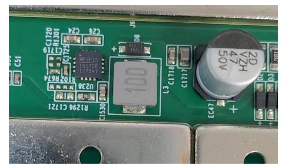
Figure 5-1

Figure 5-2
Step 4: Check the output of each group's LDO 1.2V or PLL 0.8V.
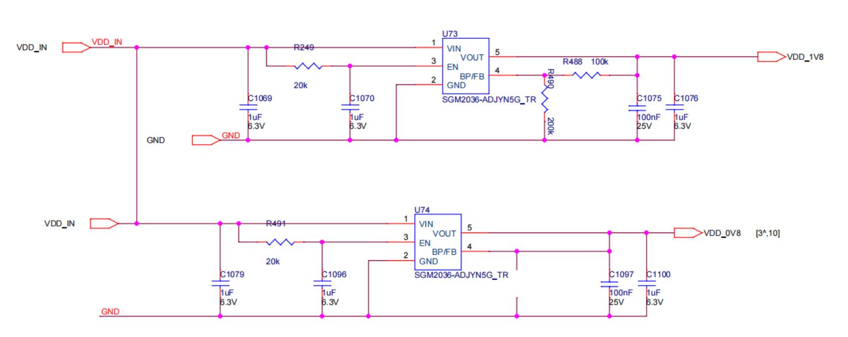
Figure 5-3
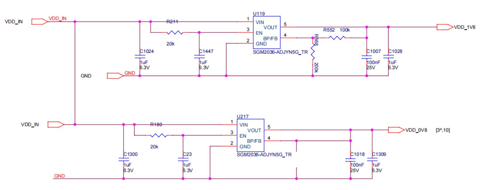
Figure 5-4
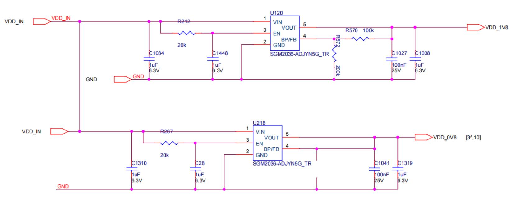
Figure 5-5
Step 5: Check the chip signal output (CLK/CI/RI/BO/RST).
Refer to the voltage value range described in the signal direction description. If there is a significant deviation in the measured voltage values, compare them with the measurements of the adjacent group for determination.
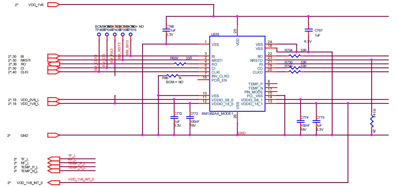
Figure 5-6
2. Phenomenon: Incomplete chip detection on the single board (PT1/PT2 stations)
a) When LCD displays ASIC NG: (0), first measure the overall voltage of the domain and check if the boost circuit 20V is normal. Then, use a short-circuit probe to short the RX test point between the 1st and 2nd chips and the 1V2 test point, and then run the chip finding program. Observe the serial port log, if still 0 chips are found, it could be one of the following situations:
a-1) Measure the voltage at the 1V2 and 0V8 test points with a multimeter to see if it's 1.2V and 0.8V. If not, it might be an issue with the 1.2V or 0.8V LDO circuit in that domain, or the main chip in this domain might not be soldered well. Or there could be a short circuit caused by the SMD filtering capacitors at 0.8V and 1.2V, or there might be issues like cold soldering, fake soldering, or material damage in the LDO circuit.
a-2) Check for any abnormalities in the U2 circuit, like false soldering in the resistors.
a-3) Check if the first chip has any unsoldered pins (it has been observed in repairs that pins appear soldered from the side, but upon removing the chip, the pins are actually not soldered at all).
b) If in step a), 1 chip is found, it indicates that the 1st chip and the preceding circuit are fine. Use a similar method to inspect the subsequent chips. For example, short the 1V2 test point between the 23rd and 24th chips and the RX test point. If the log finds 23 chips, then the previous 23 chips are fine; if it still finds 0 chips, first check if that 1V2 is normal. If it is, then the issue is with the chips after the 23rd. Continue using a binary search method to identify the problematic chip. Suppose the N chip is problematic, then shorting between the N-1 and N chips at 1V2 and RX finds N-1 chips, but shorting between the N and N+1 chips at 1V2 and RX does not find all chips.
c) Test fixture LCD display ASIC NG: X (always reports a specific chip), there are two scenarios:
The first case: (Usually, the value of the reported chip doesn't change each test). In this case, just follow the normal repair method of measuring the signal voltage and perform repair. (It could also be a collision of resistors near the chip).
The second case; the test time is almost twice as long as the good board (sometimes the value of X will change every time you test, and sometimes X = 0); at this time, the log usually has the following information (sometimes the red number is not 13, depending on which seat the test fixture is connected to); during the test, assume that the domain voltage of all the fields in front of the abnormal position is almost less than 0.3V, and the domain voltage of the back fields are almost all higher than 0.34V. This situation is caused by the chip not being soldered well; usually, 1.2V, 0.8V, RXT, and CLK are not soldered well. It is recommended to directly measure the domain voltage to locate which domain is the problem. The 1V2 and RO short-circuit methods used in section 1 can also locate the abnormal position.

Figure 5-7
3. Phenomenon: Single board Pattern NG, incomplete response of nonce data (PT2 station).
Pattern NG occurs due to significant differences in the characteristics of one chip compared to others. It has been found that the chip die is damaged, so only the chip needs to be replaced. Based on the log information, the replacement rules are:
1)Check the quality of the thermal grease printing.
2)If the chip's appearance is intact, replace the chip with the lowest response rate in each domain.
3)Swap chips with higher and lower response rates to see if the issue follows the chip. If it does, replace the chip. If not, check if the voltage in that domain is lower than normal and measure if the resistance of the chip pads is normal. If there's a difference, check if the adjacent small resistors have abnormally high resistance values. If so, replace them.
PS: It's important to note that both the domain and ASIC numbering start from 0.

Figure 5-8

Figure 5-9
4. Phenomenon: B_A X PCS (response insufficient in X chips)
Swap these few chips with those that have higher response rates in other domains to see if it is effective. If not, simply replace these chips.
5. Phenomenon: Chip testing is OK, but PT2 functional testing serial port does not stop (continuous running).
Repair method: During PT2 testing, observe the serial port print log. When the serial port starts to run continuously, use a short-circuit probe to short RX & 1.2V. Start shorting from the 1st chip, if the serial port stops running continuously after shorting, it indicates that the 1st chip is OK. Continue this method until you find the chip that, when shorted, still causes the continuous running issue. Generally, this is caused by a faulty chip, which should be replaced.

Figure 5-10
Requirements for the PT2 testing environment: The temperature for PT2 testing should be between 20 and 30 degrees Celsius. If the environmental temperature exceeds 35 degrees, the software will stop testing. Heat dissipation is required during measurement. As shown in the figure, the heat dissipation platform can be used to dissipate heat for PT1 measurements and run the DEBUG firmware.
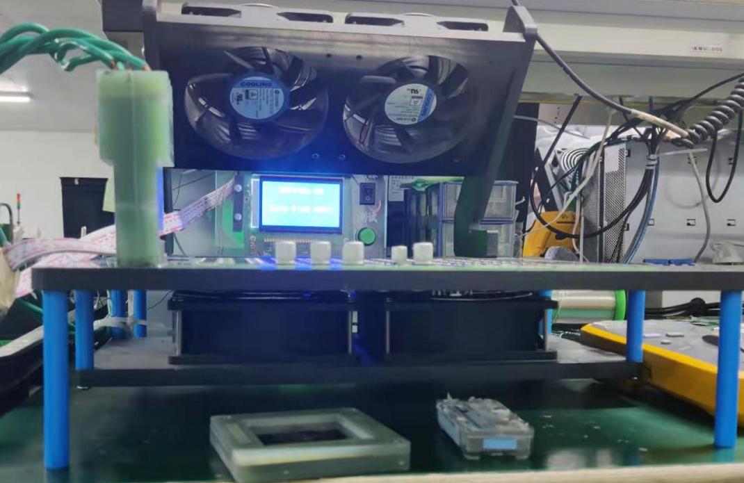
Figure 5-11
6. Chip address error (PT2)
Repair method: Replace the chip that is reporting the error.
7. For PNG where the NONCE response is low, first swap it with a good chip. If the issue follows the chip, replace the bad chip.
8. Single board OK, but complete machine loses hash rate.
1)One of the chips has erratic RX responses.
2)The LDO power supply of a certain domain is unstable, possibly due to abnormal resistance values of the resistors in series with it.
Ⅵ. Control Board Issues Leading to the Following Problems
1. The complete machine does not run
1) Check if the voltages at several output points are normal. If there is a short circuit at 3.3V, you can first disconnect U8. If it is still short-circuited, remove the CPU and measure again. For other abnormal voltages, generally replace the corresponding voltage conversion IC.
2) If the voltages are normal, please check the soldering condition of the DDR/CPU (X-RAY inspection at the production end).
3) Try to update the flash program using an SD card:
For machines that need normal startup after being flashed with a card, the following two steps are required:
a) After successful flashing, the green LED indicator will stay on. At this time, power off and restart.
b) After re-powering, wait for 30s (the time it takes to open OTP).
OTP (One Time Programmable) is a type of memory in MCU, meaning it can be programmed only once: once the program is burned into the IC, it cannot be changed or erased again.
Precautions:
If there is a sudden power cut during the OTP process or if the time is less than 30s, it may cause the control board's OTP function to fail, resulting in the control board not starting (not connecting to the network). In this case, replace U1 (the main control IC FBGA on the control board). The replaced U1 should not be used again in the 19 series.
For control boards with the OTP function activated, U1 should not be used in other series of machines.
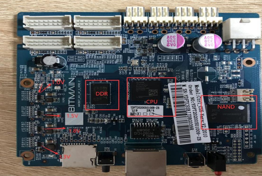
Figure 6-1
2. The whole machine cannot find an IP address
The inability to find an IP address is likely due to operational anomalies. Refer to point 1 for troubleshooting.
Check the network port, network transformer T1, and the appearance and soldering of the CPU.
3. The complete machine cannot be upgraded
Check the network port, network transformer T1, and the appearance and soldering of the CPU.
4. The complete machine fails to read hash boards or has miss chain.
A. Check the condition of the ribbon cable connections.
B. Check the components corresponding to the chain on the control board.
C. Inspect the quality of wave soldering on the connector pins and the resistors around the connector interface.
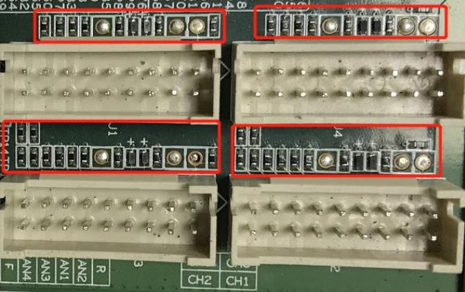
Figure 6-2
Ⅶ. Complete machine fault symptoms
1. Initial testing of the complete machine
Refer to the testing procedure document. Generally, problems that arise are due to assembly process issues or control board process issues.
Common symptoms: inability to detect IP, abnormal fan count detection, and chain detection anomalies. If anomalies occur during testing, maintenance should be conducted according to the monitoring interface and test LOG indications. The methods for repairing during initial testing and aging testing of the complete machine are the same.
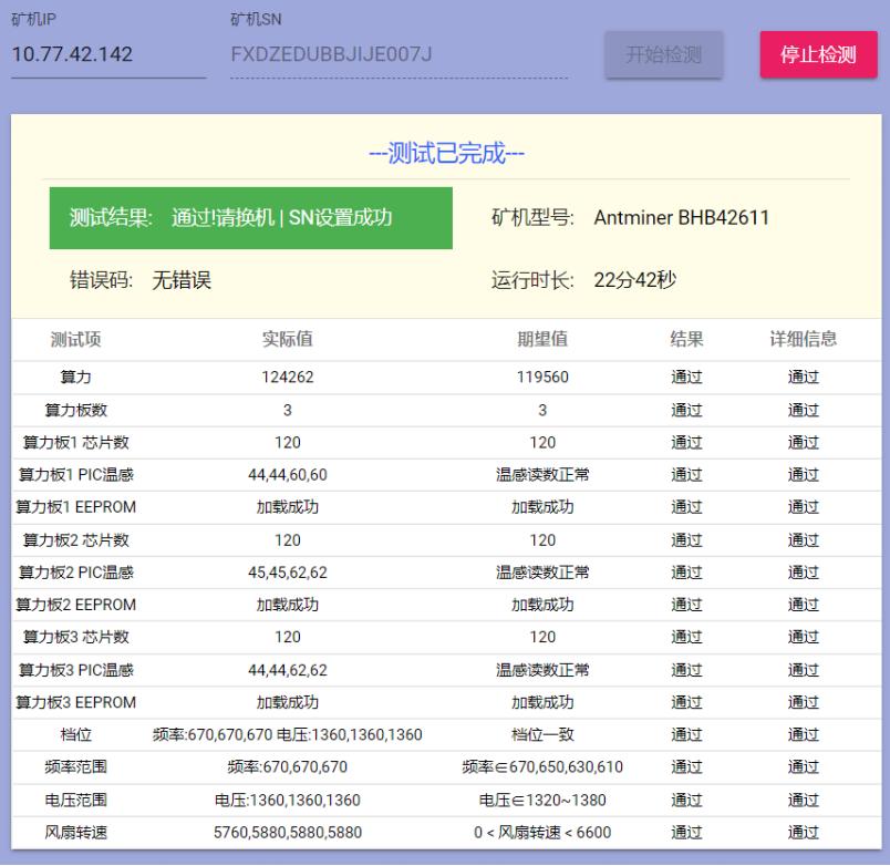
Figure 7-1
2. Aging Test: During the aging test, repairs should be based on the monitoring interface test.
1) Abnormal fan display: Check if the fan is working properly, if the connection to the control board is normal, and if there are any abnormalities in the control board.
2) Missing chain: This usually means that one of the three boards is missing. This is mostly due to problems in the connection between the hash board and the control board. Inspect the ribbon cables for any open circuit issues. If the connection is OK, perform a PT2 test on the single board to see if it passes. If it passes, it's likely an issue with the control board. If it doesn't pass, use the PT2 repair method.
3)Temperature anomaly: Generally, this refers to high temperatures. The monitoring system sets a maximum PCB temperature of 90 degrees Celsius. If it exceeds 90 degrees, the machine will alarm and not work properly. This is usually caused by high environmental temperatures or abnormal fan operation. (BHB42611 has only two temperature sensors).
4) Inability to find all chips, insufficient chip count: If the chip count is insufficient, refer to the PT1 test for repairs.
5) Loss of hash rate after running for a while, mining pool connection interrupted: Check the network.
6) Normal aging test status of good quality machines.
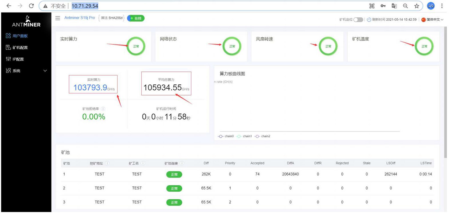
Figure 7-2
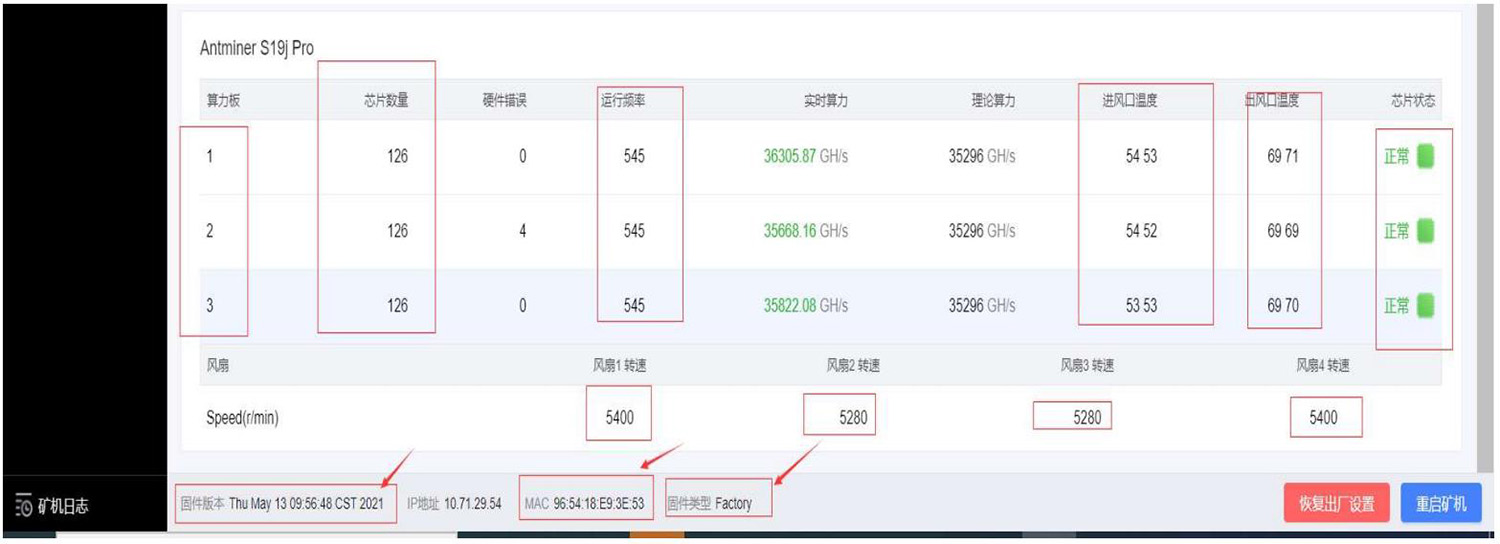
Figure 7-3
Ⅷ. Other precautions
Repair flow chart

Figure 8-1 Repair flowchart
⚫ Routine Inspection: First, visually inspect the hash board to be repaired, checking for PCB deformation or signs of burning. If present, these must be addressed first. Look for obvious signs of burnt components, components that are displaced due to impact, or missing parts. Next, if there are no visual issues, start by checking the impedance in each voltage domain to detect any short circuits or open circuits. If any are found, they must be addressed first. Then, check if each domain's voltage is around 0.32V.
⚫ After passing routine inspection (generally, short circuit testing in routine inspection is essential to prevent burning out chips or other materials when powered on), use a test fixture to check the chips and make determinations based on the results.
⚫ Based on the display results of the test fixture, start near the faulty chip and check the chip test points (CO/NRST/RX/XIN/BI) and voltages like VDD0V8, VDD1V2, etc.
⚫ Then, follow the signal direction, noting that the RX signal travels in reverse (from chip 120 to 1), while several other signals like CLK, CO, BO, RST travel forward (from 1 to 120). Locate abnormal fault points through the power sequence.
⚫ When pinpointing the faulty chip, it needs to be re-soldered. Apply flux (preferably no-clean flux) around the chip and heat each solder point of the chip pins until they melt, allowing the chip pins to re-align with the pads and re-tin. If the problem persists after re-soldering, replace the chip directly.
⚫ After repairing the hash board, it must pass the test fixture test at least twice before being considered good. First, after replacing components and allowing the hash board to cool down, test it with the test fixture and set it aside to cool again. Second, after a few minutes when the hash board has completely cooled down, test it again.
⚫ After the hash board repair is OK, maintain related repair/analysis records (repair report requirements: date, SN, PCB version, position number, cause of failure, responsibility for the defect, etc.).
⚫ After recording, assemble it into a complete machine for routine aging.
⚫ For repaired hash boards, the thermal gel must be removed and the large heat sink reprinted!
We use cookles to Improve your online experience. By continuing browsing this website, we assume you agree our use of cookies.