


Antminer S19a T19a 28611 Hash Board Repair Guide
I. Maintenance Platform/Tools/Equipment Preparation Requirements
1. Platform Requirements:
Electrostatic protective repair workbench (the workbench needs to be grounded), anti-static wrist strap, and grounding.
2. Equipment Requirements:
A constant temperature soldering iron (350℃ to 380℃), a fine tip soldering iron tip for soldering small SMD resistors and capacitors; a hot air gun, BGA rework station for chip/BGA removal and soldering; a multimeter, soldering steel needles covered with heat shrink tubing for easy measurement (Fluke recommended); oscilloscope, ethernet cable (requirements: connect to the Internet, stable network).
3. Testing Tools Requirements:
APW12 power supply (APW12_12V-15V_V1.2) and power adapter cable (DIY: use thick copper wire to connect the positive and negative terminals of the power supply to the hash board, recommend using 4AWG, copper wire length within 60cm, only for PT1 and maintenance testing); use V3.1020 control board test fixture (test fixture part number ZJ0001000001). The power supply's positive and negative terminals on the test fixture need to have discharge resistors installed, recommending using 20 Ohm, 100W or above cement resistors.
4. Repair Auxiliary Materials / Tools Requirements:
Solder paste M705, flux, PCB cleaning agent with anhydrous alcohol; PCB cleaning agent for cleaning residual flux after repair; thermal grease (specification: Fujipoly SPG-30B) for applying on the chip surface after repair; tin planting stencil, tin removal wire, solder balls (recommended ball diameter 0.4mm); when replacing a new chip, tin the chip pins before soldering to the hash board, evenly apply thermal grease on the chip surface before locking the heat sink.
5. Common Repair Spare Materials Requirements:
0402 resistors (0R, 51R, 10K, 4.7K); 0402 capacitors (0.1uf, 1uf).
II. Repair Requirements
1. When replacing chips, pay attention to the technique. After replacing any components, the PCB should not be visibly deformed. Inspect the replaced parts and their surroundings for any missing components, open circuits, or short circuits.
2. Repair personnel must possess a certain level of electronics knowledge and have over a year of repair experience, with proficient skills in soldering BGA/QFN/LGA package types.
3. After repair, the hash board must be tested twice and both results must be OK before it is considered passable!
4. Check whether tools and test fixtures are working normally. Confirm the repair station's test software parameters and the version of the test fixtures.
5. Testing of the chip replacement requires first checking the chip, and if it passes, then conducting a functional test. The functional test must ensure that the small heat sink is soldered OK and the large heat sink is properly installed (thermal grease must be evenly applied before installing the large heat sink), and the cooling fan is at full speed. For chassis cooling, insert 2 hash boards to form an airflow channel during production's single-side test to ensure airflow formation (important).
6. When measuring signals, use 4 fans for cooling, keeping the fans at full speed.
7. When powering on the hash board, the power supply's negative copper wire must be connected first, followed by the positive copper wire, and finally, the signal ribbon cable. For disassembly, reverse the order: first remove the signal ribbon cable, then the positive copper wire, and finally the negative copper wire. Not following this sequence can easily damage U1, U2 (making it hard to find complete chips). Before testing the pattern, the repaired hash board must cool down, or it will lead to a test PNG.
8. When replacing a new chip, the pins and solder paste must be printed to ensure that the chip is pre-tinned and then soldered to the PCBA for repair.
9. The repair end's test fixtures all use Test_Mode mode and are tested using a scanning mode. After passing the test, the production side starts from the first station of the testing line and proceeds with normal assembly and aging (assemble according to the same level).
III. Test fixture Production and Precautions
1. The test fixture and its accompanying fixtures should facilitate cooling of the hash board and make it easy to measure signals.
2. Material pickup number: ZJ0001000001 for the testing jig.
3. For the first use of the 28611 series test fixture, program the SD card to update the FPGA on the control board of the test fixture. After unzipping, copy the files to the SD card and insert the card into the test fixture's slot; Power on for about 1 minute and wait for the indicator light on the control board to double flash 3 times before the update is completed; (Failure to update may result in the test consistently reporting a particular chip as defective).

Figure 3-1
4. Create the testing SD card as needed. For testing chips with a single-sided heat sink, simply unzip the package and prepare the SD card directly;
Note: Sometimes the software configuration file, the Config file, included in the original package may not necessarily be for PT1, so it is crucial to confirm whether it is the PT1 configuration file. Do not connect an ethernet cable or barcode scanner during PT1 testing.
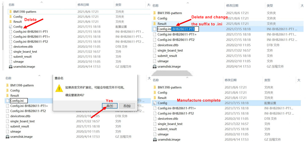
Figure 3-2
5. Create the testing SD card as needed for double-sided heat sink 8x Pattern testing, as indicated in the following diagram; during PT2 testing, a barcode scanner and ethernet cable need to be connected.


Figure 3-3
IV. Principle Overview
1. 28611 Hash Board Working Structure:
The hash board is composed of 72 BM1398 chips, divided into 9 groups (domains), each group consisting of 8 ICs. The working voltage of the BM1398 chips used in the 28611 hash board is 1.3V. Due to the series connection of chips, the signal transmission process will attenuate, so 0.8V signals are supplied from both ends respectively. The 9th group is powered by a boost circuit U12, which outputs 22V that is then outputted as 1.8V by linear regulators (U169, U170). This output voltage supplies LDO (U123, U133) with 0.8V. From the 8th group to the 1st group, VDD 13V supplies 1.8V and 0.8V through LDO, with the voltage decreasing by 1.3V for each domain moving backwards, as shown in Figure 4-1.
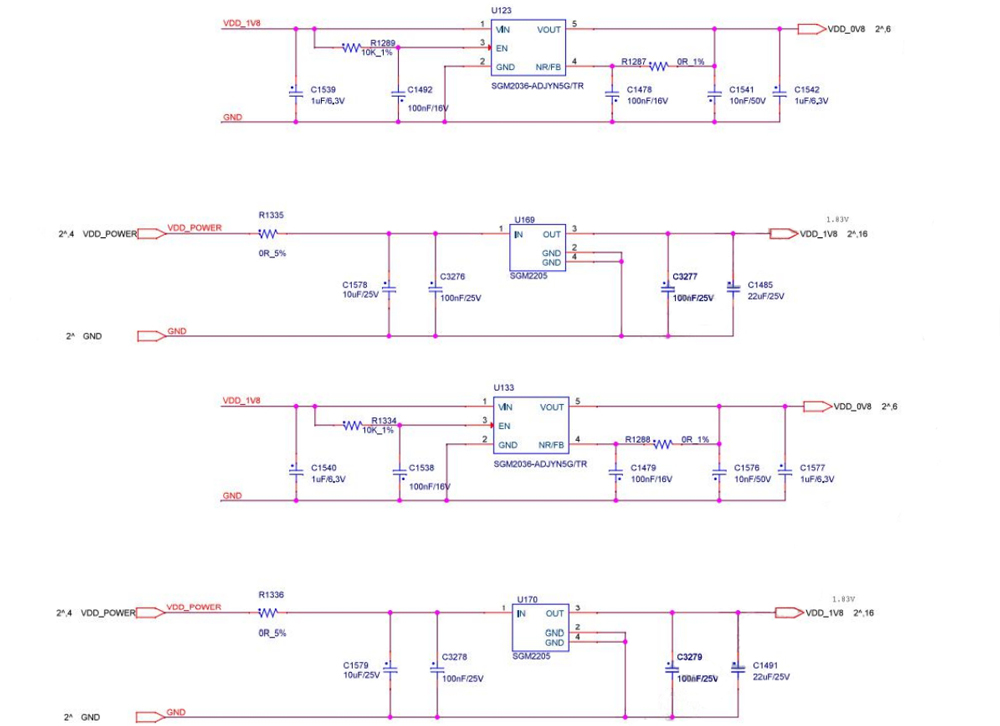
Figure 4-1 (Group 9)
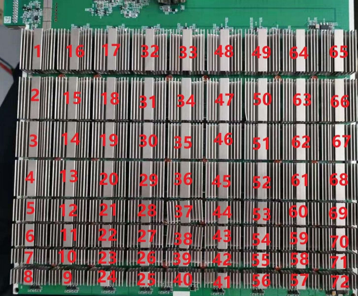
Figure 4-2
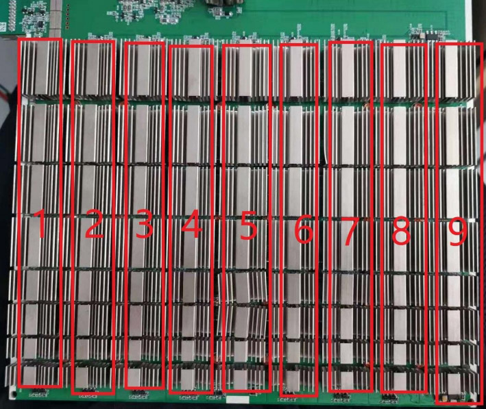
Figure 4-3
2. 28611 Hash Board Boost Circuit:
The boost is powered by the power supply from 13V to 22V, as shown in Figure 4-5.
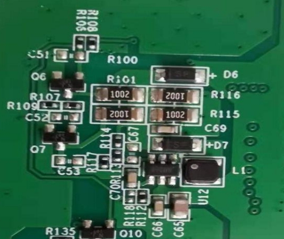
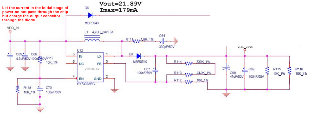
Figure 4-4
3. 28611 Chip Signal Direction:
CLK (XIN) signal direction: generated by Y1 and Y2 (bit mark) 25MHZ crystal oscillator, transmitted from chip 01 to chip 72; the voltage is about 0.9V.
RST and CI signal direction: entering from IO interface pin 3 (3.3V) and after conversion by level shifter IC U1 - U2 - U4, it transmits from chip 01 to chip 72; voltage is 0V when IO cable is not connected, and 1.8V during operation.
RX (RI, RO) signal direction: from chip 72 to chip 01, return to the control board via U1 to pin 8 of the signal cable terminal; voltage is 0.3V when IO cable is not connected, and 1.8V during operation.
BO (BI, BO) signal direction: from chip 01 to chip 72. Use a multimeter to measure 0V..
4. Overall Machine Architecture:
The entire machine primarily consists of 3 hash boards, 1 control board, an APW12 power supply, and 4 cooling fans, as shown in Figure 4-6.
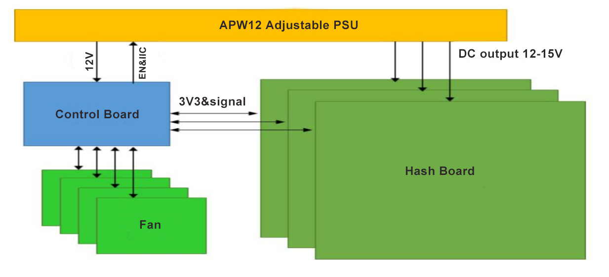
Figure 4-6
V. Common Hash Board Faults and Troubleshooting Steps
1. Symptom: Single board test detects zero chips (PT1/PT2 stations).
First step: Check the power supply output first. Please inspect the voltage at the parts circled in Figure 5-1.
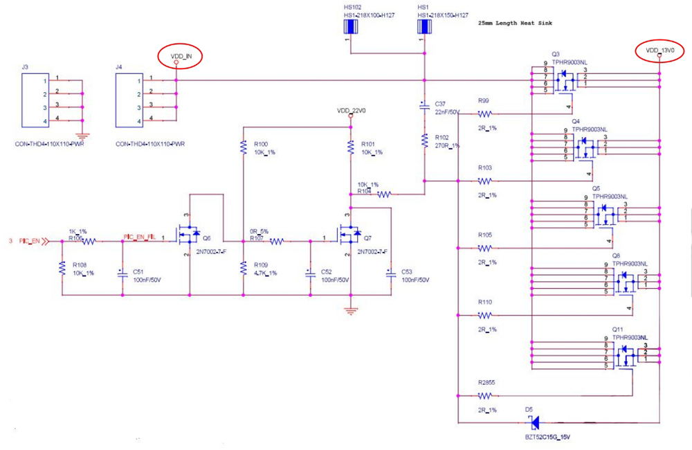

Figure 5-1
Second Step: Check the voltage domain outputs. Each voltage domain should output approximately 1.3V. If there is a 13V supply, there generally should be domain voltage. Prioritize measuring the output at the hash board's power terminals and check if there is any short circuit in the MOS (measure the resistance between pins 1, 4, and 8). If there is a 13V supply but no domain voltage, continue with further investigation.

Figure 5-2
Third Step: Check the PIC Circuit
Measure whether there is output at pin 11 of U6 (the output value needs to be measured). If there is an output, continue investigating further. If there is no output, please check the connection status of the test fixture ribbon cable to the hash board is OK, and consider reprogramming the PIC.
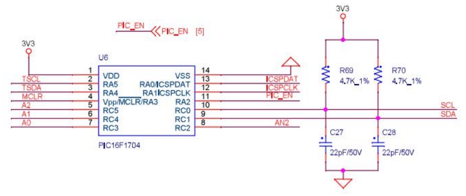
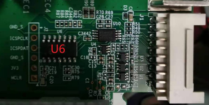
Figure 5-3
PIC Programming Steps:
1) Hash Board PIC Programming.
Program: 20200101-PIC1704-BM1398-V89.hex
Download and use the programming tool: PICkit3. The pin 1 of PICkit3's ribbon cable corresponds to pin 1 of J3 on the PCB. It's necessary to connect pins 1, 2, 3, 4, 5, and 6.
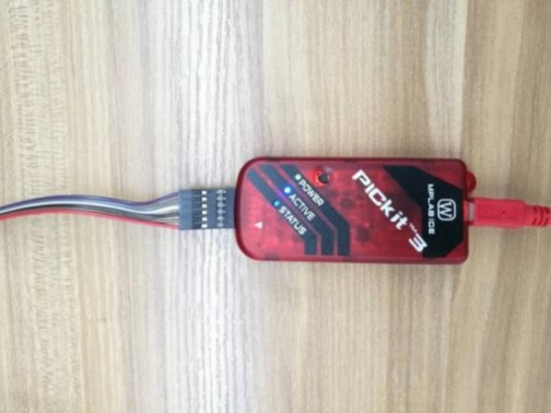
Figure 5-4
2) Programming Software:
Open MPLAB IPE and select the device: PIC16F1704. Click on "power" to choose the power supply method. Then click on "operate".
Step 1: Select "file" to locate the .HEX file you want to program.
Step 2: Click on "connect" to ensure a successful connection.
Step 3: Click the "program" button. After completion, click "verify". A message indicating verification completion confirms that the programming was successful.

Figure 5-5
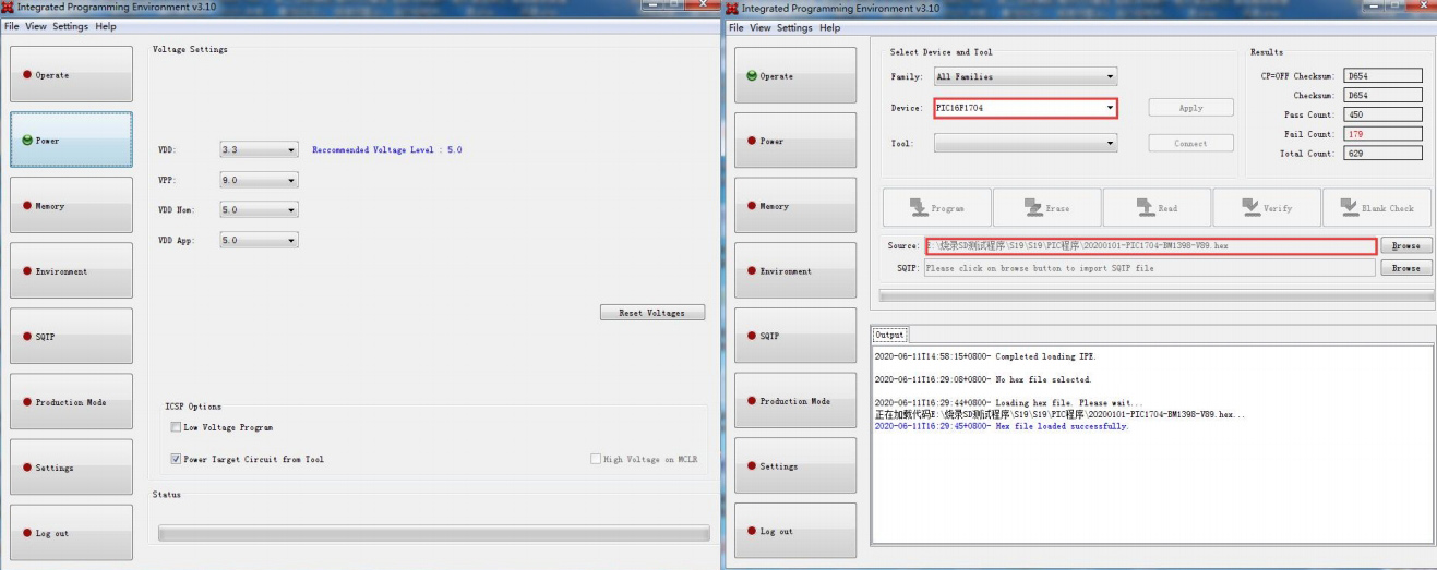
Figure 5-6
Step 4: Check the boost circuit output. Test at C69 as shown in Figure 5-7 to measure 22V voltage.
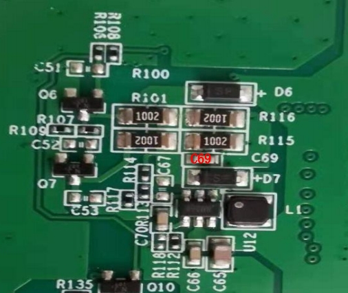
Figure 5-7
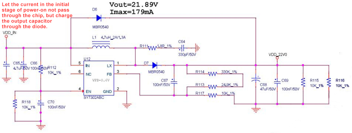
Figure 5-8
Step 5: Check the output of each group's LDO for 1.8V or the PLL for 0.8V output.
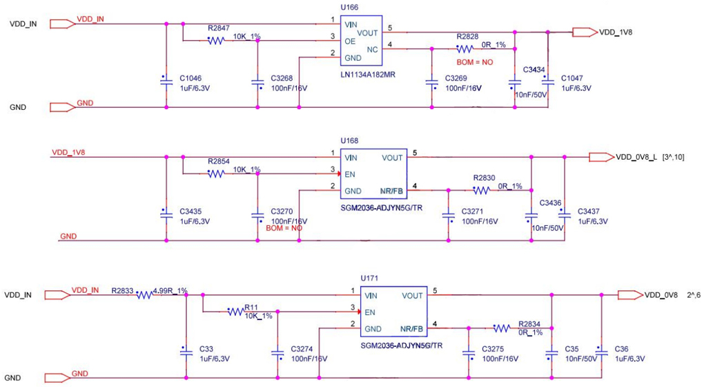
Group 1 – Group 8
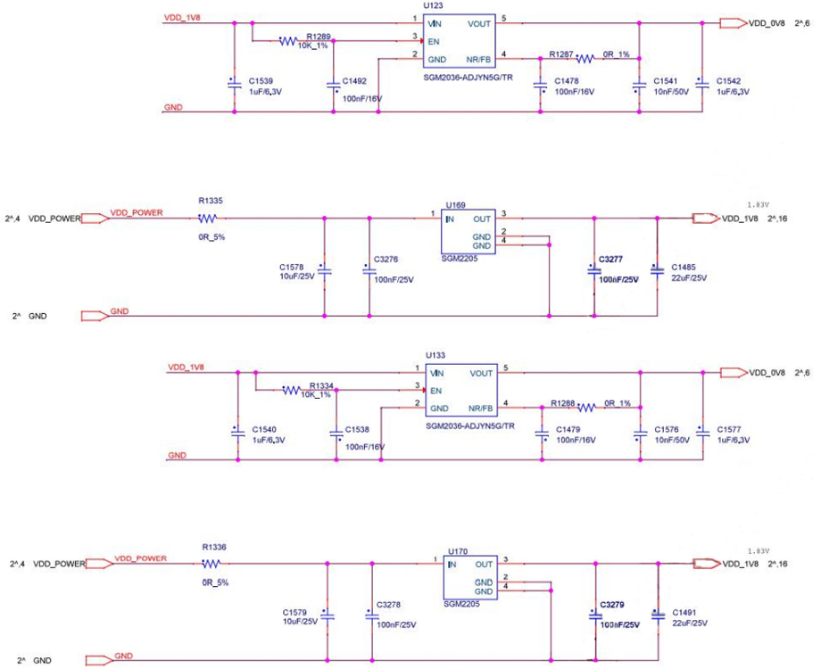
Group 9
Figure 5-9
Step 6: Check the chip signal outputs (CLK, CI, RI, BO, RST).
Refer to the described voltage ranges for signal direction. If there is a significant deviation in measured voltage values, compare them with the values from adjacent groups to decide.
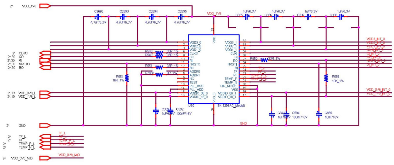
Figure 5-10
When the test fixture LCD screen displays "EEPROM NG," check whether U10 is soldered properly.

Figure 5-11
When the test fixture LCD screen displays "PIC sensor NG," indicating abnormal temperature readings, troubleshoot using the following steps:
Check whether the temperature sensors at U136, U145, U137, U142 are soldered properly, as shown in Figure 5-12. Also, verify that the VDD power to the temperature sensors is normal. Inspect the soldering quality of the chips connected to the temperature sensors and the small heat sink; deformation in the material of the large heat sink can lead to poor chip cooling, affecting temperature differences.

Figure 5-12
2. Phenomenon: The single board detection chip is incomplete (at PT1/PT2 stations)
a) LCD Display ASIC NG: When (0), first measure the total voltage of the domain and check if the 22V boost circuit is normal, and then use a short-circuit probe to short-circuit the RO test point between the first and second chips. Then run the chip-finding program. Check the serial port log; if still 0 chips are found, then it could be one of the following situations:
a-1) Use a multimeter to measure whether the voltage at the 1V8 and 0V8 test points is 1.8V and 0.8V, respectively. If not, it could be that the 1.8V and 0.8V LDO circuits in that domain are abnormal, or the two ASIC chips in this domain are not soldered well, mostly caused by a short circuit in the 0.8V and 1.8V SMD filter capacitors (measure the resistance of related SMD capacitors on the aluminum substrate).
a-2) Check if there are any abnormalities in the circuits of U1, U2, and U4, such as virtual soldering of resistors.
a-3) Measured with a multimeter is 0V. Check whether the pins of the first chip are not soldered properly (it was found during maintenance that the pins were tinned when viewed from the side, but after removing the chip, it was found that the pins were not stained with tin at all).
b) If, in step a), 1 chip can be found, it means the first chip and the previous circuit are fine. Similarly, proceed to check the subsequent chips. For example, short the 1V8 test point and the RO test point between the 38th and 39th chips. If the log can find 38 chips, then the first 38 chips are fine; if still 0 chips are found, first check if the 1V2 is normal. If normal, then the problem lies with the chips after the 38th. Continue to use the binary search method to identify the faulty chip. Suppose the Nth chip is faulty, then shorting the 1V8 and RO between the N-1 and N chips will allow the N-1 chips to be found, but shorting the 1V8 and RO between the N and N+1 chips will result in not all chips being found.
c) LCD Display ASIC 71: When (reporting 71), it indicates that the hash board can detect 72 chips at a baud rate of 115200, but only 71 chips are found at a baud rate of 12M. There is 1 chip not found at 12M baud rate;
Repair method: Use the binary search method, and with a short-circuit probe, (for example) short the 1V8 test point and the RO test point between the 38th and 39th chips. If the log can find 38 chips, then the first 38 chips have no issues; if shorting the 47th chip results in the log reporting 46 chips, it indicates that the 47th chip cannot be detected. If there are no apparent issues upon visual inspection, generally replacing the 47th chip will suffice.
d) LCD Display ASIC NG: When it consistently reports a specific chip, there are two scenarios:
d-1) The first scenario; (usually, the reported chip value does not change with each test). In such cases, proceed with the repair using the standard method of measuring signal voltages.
d-2) The second scenario; (B_A) the test duration for the problematic board is almost double that of an OK board (sometimes, the X (gear) value may change with each test);
Remove the heatsink to check if the chip has any die cracks or soldering issues;
According to the log of PT2, swap the chip with the highest nonce value and the chip with the lowest nonce value;
Remove the chip with a low nonce and replace it with a new chip.
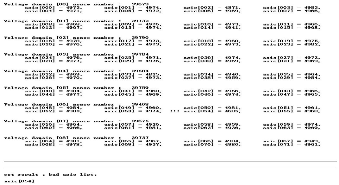
Figure 5-13
d-3) Currently, in production and repair, most issues found are due to micro short circuits between signals (0 to several hundred ohms) caused by too small resistance values of chip pins. First, try re-soldering with a hot air gun to see if it resolves the issue.
3. Phenomenon: Single board Pattern NG, meaning the reply nonce data is incomplete (at PT2 station)
Pattern NG occurs due to significant differences in characteristics between one chip and others, leading to issues. There have been instances where chip die damage was discovered, so simply replacing the affected chip suffices. According to log information, the replacement rule is: if there is no visible damage to the chip, replace the chip with the lowest nonce in each domain. As shown in one of the test logs below, it is evident that the nonce of asic[36][37][43] is relatively low. Since 36 and 37 are in the same domain, replace the one with the lower nonce between 36 and 37. Also, replace chip 43.
PS: It is important to note that the numbering for domains and asics starts from 0.
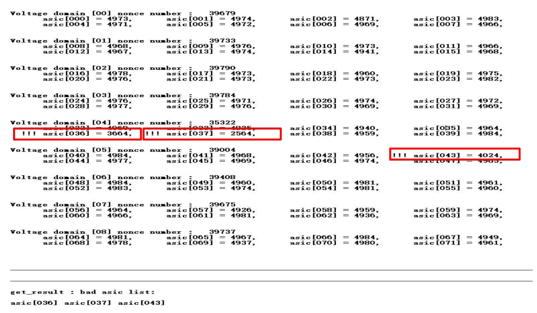
Figure 5-14
4. Phenomenon: Chip testing OK, but PT2 functional testing serial port does not stop (continues running).
Repair method: During PT2 testing, observe the serial port printing log. When the serial port starts to run continuously, use a short-circuit probe to short RO & 1.8V, starting from the first chip. If the serial port stops running continuously after short-circuiting, it indicates the first chip is OK. Use this method to identify the chip that, when short-circuited, still causes the continuous running issue. Usually, it's caused by a faulty chip, and replacing it should resolve the issue.
Requirements for the PT2 testing environment: The temperature for the PT2 testing environment should be between 20°C to 30°C. The software will stop testing if the environmental temperature exceeds 35°C.
Requirements for the PT2 test power supply: For the PT2 test fixture power supply, under a load of 1500W (when testing a single board), the actual output voltage must not be lower than 0.03V below the configuration file setting. (For example, if the configuration file requires a test production of 15V, then the power supply output voltage under a 1500W load must not be lower than 14.97V).
Ⅵ. Control Board Issues Leading to the Following Problems
1. The whole machine does not run
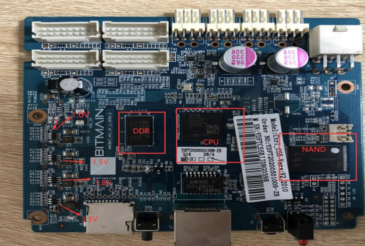
1) Check if the voltage at several output points is normal. For a 3.3V short circuit, first disconnect U8. If it still shows a short circuit, remove the CPU and then measure again. For other voltage anomalies, generally replace the corresponding voltage conversion IC.
2) If the voltage is normal, check the soldering condition of DDR/CPU (X-RAY inspection on the production side).
3) Try updating the flash program with an SD card;
4) To normally start a machine that has been flashed with a control board, the following two steps are needed:
a) After a successful flash, the green LED indicator will stay on. At this point, power off and restart;
b) After re-powering, wait for 30s (the time it takes to open OTP).
c) OTP (One Time Programmable) is a type of memory in MCU, meaning it can be programmed only once: once the program is burned into the IC, it cannot be changed or erased again.
Precautions:
1) If the power is suddenly cut off during the OTP process or if the time does not reach 30 seconds, it will cause the OTP function activation of the control board to fail, resulting in the control board not starting (not connecting to the network). In such cases, U1 (the main control IC FBGA of the control board) needs to be replaced. The replaced U1 cannot be used on the 19 series again.
2) Control boards that have undergone the OTP function activation cannot use their U1 on other series models.
2. The whole machine cannot find IP
The inability to find an IP is likely due to abnormal operation. Refer to point 1 for troubleshooting.
Check the appearance and soldering condition of the network port, network transformer T1, and CPU.
3. The whole machine cannot be upgraded
Check the appearance and soldering condition of the network port, network transformer T1, and CPU.
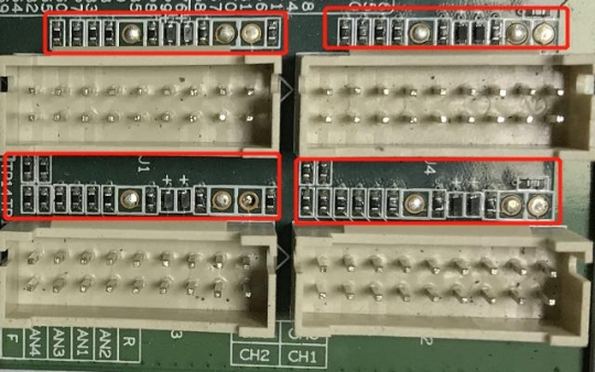
4. The whole machine fails to read the hash board or has a missing chain
A. Check the connection status of the ribbon cable.
B. Check the parts of the control board corresponding to the chain.
C. Check the wave soldering quality of the header pins and the resistance around the plug-in interface.
Ⅶ. Whole Machine Fault Symptoms
1. Initial Testing of the Whole Machine
Refer to the testing process document. Problems generally arise from assembly process issues or control board process issues.
Common symptoms include: unable to detect IP, abnormal fan speed detection, and abnormal chain detection. If abnormalities occur during testing, repairs should be made according to the monitoring interface and test LOG indications. The methods for repairing issues found during initial testing and aging tests are consistent.
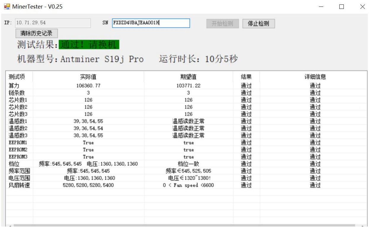
Figure 7-1
2. Aging Test: During the aging test, repairs should be conducted based on the monitoring interface test. For example:
1) If the fan display is abnormal - it is necessary to check whether the fan is working properly, whether the connection to the control board is normal, and whether there are any anomalies with the control board itself.
2) Missing chain: A missing chain means that at least one of the three boards is missing. In most cases, this issue arises from a problem with the connection between the hash board and the control board. Inspect the ribbon cable for any open circuit phenomena. If the connection is OK, you can proceed to test the single board with a PT2 test to see if it can pass. If it passes, it can generally be concluded that the issue lies with the control board. If the test fails, then use the repair method for PT2 to carry out repairs.3) Abnormal Temperature: Generally, the issue is high temperature. Our monitoring system sets the maximum PCB temperature at no more than 90 degrees Celsius. If the temperature exceeds 90 degrees, the machine will alarm and cannot work normally. This is usually caused by an excessively high ambient temperature, and abnormal fan operation can also cause temperature anomalies.
4) Incomplete Chip Detection (the machine can still boot, but the hash rate is 2/3 or 1/3 of the normal value) Insufficient Number of Chips: If there are not enough chips, refer to the PT2 testing and repair process.
5) After running for a period of time, there is no hash rate and the mining pool connection is interrupted. Check the network;
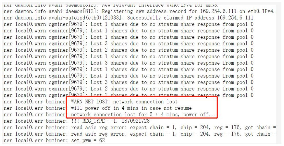
Figure 7-2
6) The aging test status of a normally functioning machine.
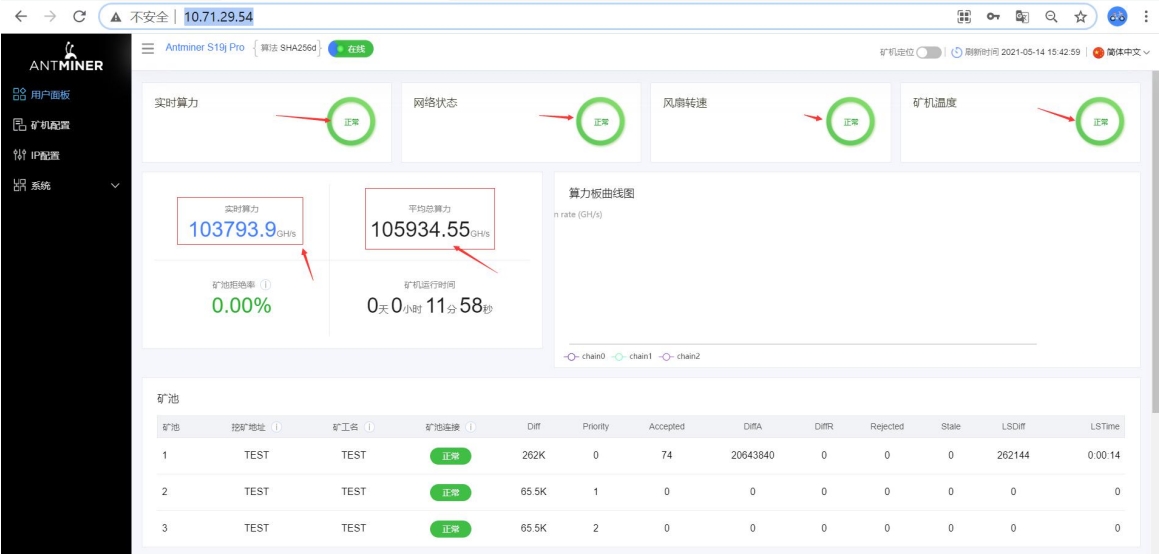
Figure 7-3
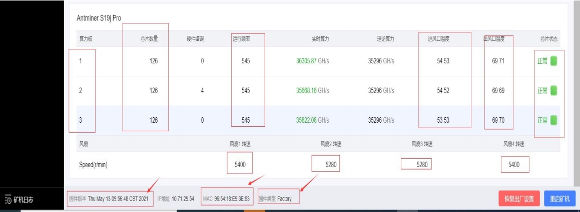
Figure 7-4
7) For a single board that tests OK but then shows a low hash rate after being assembled into a complete machine. As shown in the figure below, the first board stops producing a hash rate after running for about 3 minutes. The specific analysis method is as follows:
First, perform a single board PT2 test to see if this board is OK. If the test does not detect all chips, then repair the single board. If the test is normal and the gear position is OK, then take this board out separately and use the test fixture to transfer it into a DeBug master program for mining, adjusting the fan speed to 95%. Adjust the voltage and frequency to the whole machine's working voltage and frequency, and let the machine mine to see if the machine experiences a drop in hash rate. If the machine still drops hash rate, then reduce the frequency to 200M while keeping other conditions the same. Let the machine mine to see if the hash rate drops and if the hash board shows an X. If it still shows an X and drops hash rate, then remove the heat sink from the hash board and continue mining. When the hash rate drops, measure whether the domain voltage is normal. Generally, the domain voltage will be abnormal in the problematic domain. Then measure the RO signal to see where the RO signal is interrupted. If the RO signal is lost, it is generally because the chip is short-circuited or damaged after being soldered.
Ⅷ. Other Precautions
Repair flowchart

Figure 8-1 Repair Process Flowchart
1. Routine Inspection: First, visually inspect the hash board to be repaired for any PCB deformation or signs of burning, which must be addressed before proceeding. Check for parts with clear signs of burning, displacement due to impact, or missing components. Next, if there are no visual issues, check the impedance of each voltage domain to detect any short circuits or open circuits. Any issues found must be addressed first. Then, verify that each domain voltage is approximately 0.32V.
2. After passing routine inspection (routine short circuit detection is essential to prevent damage to chips or other materials when powered on), use a test fixture to perform chip detection and determine the fault based on the test results.
3. Based on the display results from the test fixture, start near the faulty chip and test the chip test points (CO/NRST/RO/XIN/BI) as well as voltages like VDD0V8 and VDD1V2.
4. Further, based on the direction of signal flow, except for the RO signal which is transmitted in reverse (from the 72 to 1), CLK, CO, BO, RST are transmitted forward (from 1 to 72). Identify the abnormal fault point by following the power supply sequence.
5. When pinpointing the faulty chip, it should be re-soldered. The method involves adding flux around the chip (preferably no-clean flux), then heating each pin of the chip to a molten state to facilitate re-mating of the chip pins with the solder pads and reflowing the solder. This aims to achieve a re-soldering effect. If the fault remains the same after re-soldering, the chip should be replaced directly.
6. After repairing the hash board, it must pass the test fixture testing at least twice before being deemed a good product. The first test is conducted after replacing parts and allowing the hash board to cool down. After it passes, set it aside to cool further. The second test is conducted a few minutes later, once the hash board has completely cooled down, to perform another test.
7. After the hash board is successfully repaired, it is necessary to maintain detailed repair/analysis records (the repair report should include: date, SN, PCB version, location, cause of failure, and attribution of responsibility). These records are crucial for feedback to production, after-sales service, and R&D.
8. Once the records are completed, the unit should be reassembled and put through routine aging as a complete machine.
9. Repaired good products on the production side must start from the first station of production (at least must be checked for appearance and start from the PT1/PT2 testing stations) before moving through the production line!
10. For hash boards that have been repaired, the thermal conductive gel must be removed, and the large heat sinks must be reprinted before they can proceed through the production line!
We use cookles to Improve your online experience. By continuing browsing this website, we assume you agree our use of cookies.