


Antminer S19K Pro BHB56902 Hash Board Repair Guide
I. Maintenance Platform/Tool/Equipment Preparation Requirements
1. Platform Requirements
Anti-static repair workbench (the workbench must be grounded), anti-static wrist strap and grounding.
2. Equipment Requirements
Thermostatic soldering iron (350-380 degrees Celsius), fine-tip soldering iron tip for soldering small SMD resistors and capacitors; hot air gun, BGA rework station for chip/BGA removal and soldering; multimeter, soldering steel needles covered with heat-shrink tubing for easy measurement (Fluke recommended); oscilloscope, ethernet cable (Requirements: for Internet connection, stable network).
3. Testing Tool Requirements
APW12 power supply, power adapter cable (DIY: connect the positive and negative terminals of the power supply to the hash board using thick copper wires, recommended 4AWG, with copper wire length within 60cm, limited to PT1 and repair testing use); test fixture for hash boards using V2.1 or V2.3 control boards (test fixture part number ZJ0001000004). The power positive and negative terminals of the test fixture need to have discharge resistors installed, recommend using 20 Ohm, 100W or higher cement resistors.
4. Repair Auxiliary Materials/Tool Requirements
Solder paste, flux, board cleaning liquid mixed with anhydrous alcohol; board cleaner for cleaning flux residues after repairs; thermal conductive silicone grease for applying on the chip surface after repairs; reballing stencil (for 6mm*7mm chip size), desoldering braid; when replacing new chips, it is required to tin the chip pins before soldering them to the hash board, evenly apply thermal conductive gel on the chip surface before locking the large heatsink.
5. Common Repair Spare Material Requirements
0402 resistors (0R, 33R, 51R, 10K, 4.7K); 0402 capacitors (0.1uf, 1uf)
SMD resistor, 33Ω, 1%, 1/20W, R0201 (0603)
Resistor, 10K, +/-1%, 1/16W, 0402
Resistor, 0Ω, 5%, 1/16W, 0402
SMD ceramic capacitor, 100NF, 6.3V, 10%, X5R, C0201 (0603)
II. Repair Requirements
1. When replacing chips, pay attention to the technique. After replacing any components, the PCB should not be noticeably deformed. Check that there are no missing components, open circuits, or short circuits in the replaced parts and their surroundings.
2. Repair personnel must possess a certain level of electronic knowledge and have more than one year of repair experience, with proficient mastery of BGA/QFN/LGA packaging soldering techniques.
3. After repairs, the hash board must be tested more than twice and be OK before it can pass.
4. Check that tools and test fixture are working properly, confirm the repair station test software parameters, and test fixture versions, etc.
5. After repairing and replacing chips, testing needs to first pass PT1 chip detection, then proceed to functional testing. Functional tests must ensure that the BSM radiator is soldered OK before testing PT3. When using the chassis for heat dissipation, 2 hash boards must be inserted at the same time to form an airflow channel, and single-sided testing at the production end must also ensure that an airflow channel is formed (important).
6. When measuring signals, use 4 fans to assist with cooling, keeping the fans at full speed.
7. When powering on the hash board, the power supply's negative copper wire must be connected first, followed by the positive copper wire, and finally, the signal ribbon cable. When disassembling, the order must be reversed: first disconnect the signal ribbon cable, then the positive copper wire, and finally the negative copper wire. Failing to follow this order can easily cause damage to components like U1 and U2 (missing chips). Before testing the pattern, the repaired hash board must be cooled down; otherwise, it may lead to a test failure (PNG).
8. When replacing new chips, print pins and solder paste must be applied to ensure the chip is pre-tinned before being soldered onto the PCBA for repair.
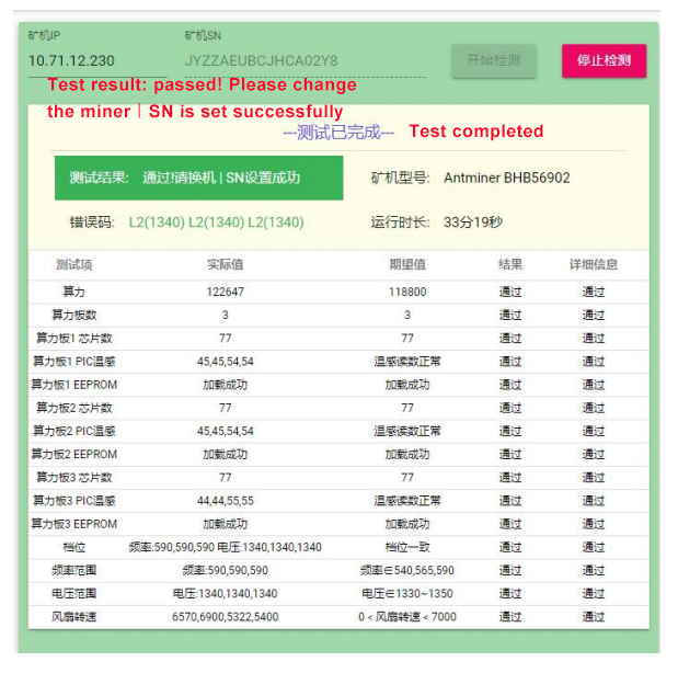
9. All testers on the repair side use Test_Mode and are tested with scan mode. After passing the test, the production side starts from the first station of the test cable and proceeds with normal assembly and aging (assembled at the same level).
10. For the BHB56902 model, the chip uses BSM technology, which means the chip surface is copper-plated, and the heatsink is directly soldered to the chip using tin. During repairs, it's required first to remove the heatsink from the chip. Adjust the hot air gun temperature to 400 degrees Celsius, position the nozzle about 0.5cm above the heatsink, and heat for 15 seconds to remove the heatsink. Then, use the same temperature and method to blow on the heatsink on the opposite side of the chip. Using the same temperature and time, you can remove the heatsink on the opposite side of the PCBA. Finally, solder the chip using the conventional method.
11. For PT1 repairs and chip replacements, or components around the chip, it is essential to clean the chip surface of any residual flux. Otherwise, during the BSM phase, it could lead to insufficient solder and abnormal soldering.
III. Test fixture Fabrication and Precautions
Test fixture should facilitate the cooling of the hash board and make it easy to measure signals.
1. Part number: ZJ0001000004 Test fixture.
2. For the first use of the 19 series test fixture, an SD card is used to flash the program for FPGA updates on the test fixture control board. After decompressing, copy it to the SD card and insert the card into the jig slot; power on for about 1 minute and wait for the control board indicator light to flash twice, three times to complete the update; (failure to update may result in consistent reporting of a specific chip defect during testing).

Figure 3-1
3. For making an SD card without heatsink: Use the PT1 program for repair that requires scanning. As illustrated in the screenshot explanation, delete the default config.ini file, and testing must be conducted via scanning. During measurement, technicians need to provide cooling to the PCBA to prevent the board from overheating during testing and measurement processes.
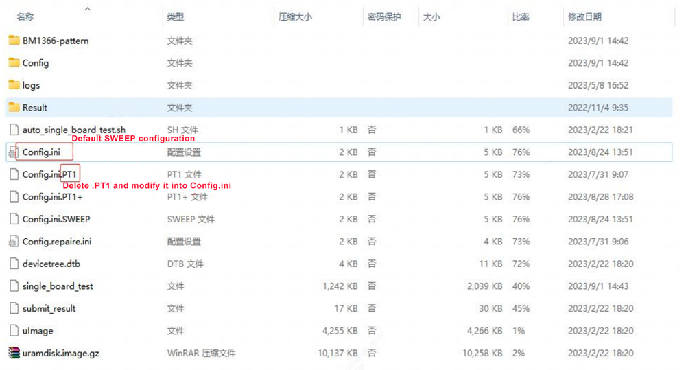
Figure 3-2
IV. Overview of Principles
1. BHB56902 Hash Board Working Structure:
The hash board consists of 77 BM1366BS chips, divided into 11 groups (domains), each group made up of 7 ICs. The BM1366 chips used in the BHB56902 hash board operate at a domain voltage of approximately 1.15V. The 10th and 11th groups (2 groups in total) are powered by 19V outputted from the boost circuit U178 to MP2019, which supplies power to LDOs via MP2019 U166,U163, resulting in LDO outputs of 1.2V and 0.8V for these two domains (Figure 4-5), whereas the supply for the remaining domains' LDOs comes from the voltage input of the previous domain, enabling them to output 1.2V and 0.8V (Figure 4-6).
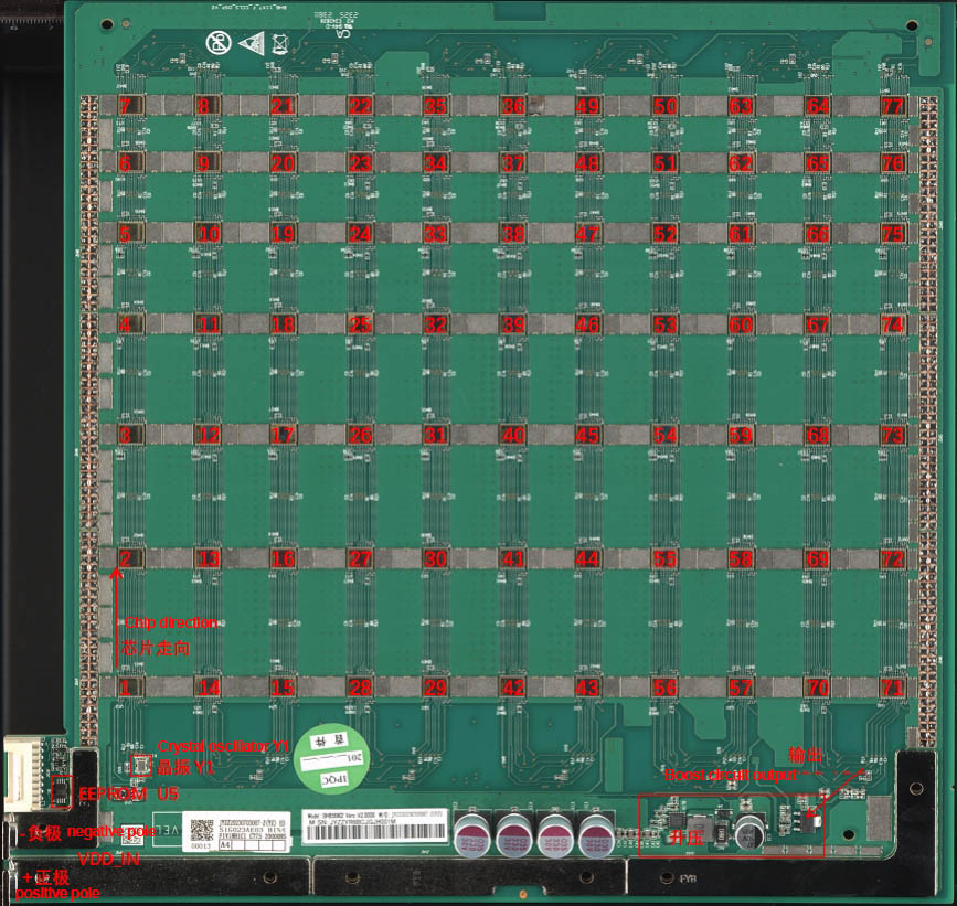
Figure 4-1
2. Temperature circuit: It consists of two temperature sensors on the BOT side, one at the air inlet and one at the air outlet, powered by 3.3V. They are connected to the J450 connector through the I2C bus SCL, SDA. If there's a temperature anomaly, first determine whether it's at the inlet or the outlet and troubleshoot the corresponding circuit. The schematic is shown in Figure 4-3.
3. Comparison between BHB56902 Hash Board and the 42612 Model: The BHB56902 hash board adds 10 level shifters to perform addition operations on signals, used from the second domain to the last, as shown in the diagram with a blue frame. Level shifters 0-9 are powered by the voltage of the previous domain (Figure 4-4).
4. Each 1366 chip cooling: Every 1366 chip has its own heatsink, which needs to be well soldered on both sides. Poor contact can affect cooling, leading to a sweep frequency PT NG.
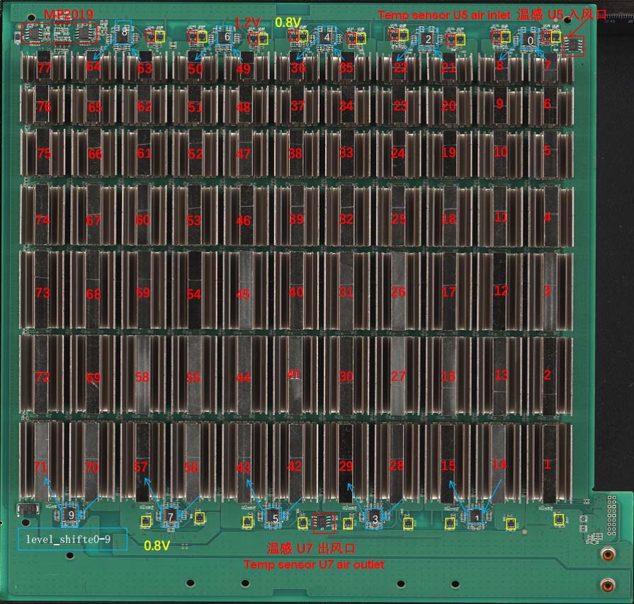
Figure 4-2
Temperature sensing schematic diagram:
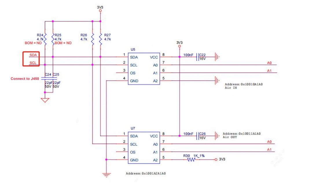
Figure 4-3
level_shifter IC schematic diagram (screenshot of 1):
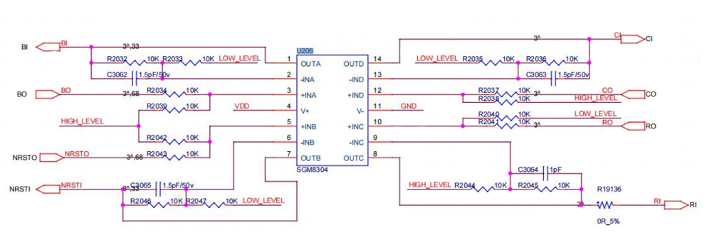
Figure 4-4
MP2019 provides 1.2V & 0.8V LDO power supply schematic diagram (screenshot of 1 group):
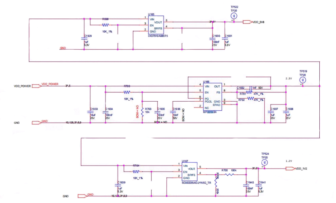
Figure 4-5
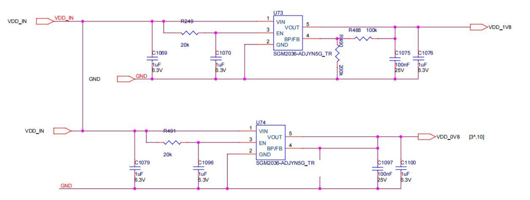
0.8V & 1.2V LDO schematic diagram (screenshot of 1 group):
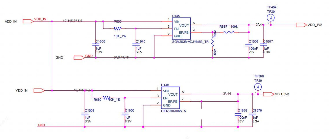
Figure 4-6
The boost is powered by the supply from 15V to 19V, as shown in Figures 4-7 and 4-8.
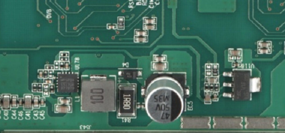
Figure 4-7

Figure 4-8
5. Signal routing for the chip on the BHB56902 hash board:
CLK (XIN) signal flow: Generated by the Y1 25MHz crystal oscillator, transmitted from chip 01 to chip 77.
RST signal flow: Enters from pin 3 of the IO port, then transmitted from chip 01 to chip 77.
CI signal flow: Enters from pin 7 of the IO port, then transmitted from chip 01 to chip 77.
RX (RI, RX) signal flow: From chip 77 to chip 01.
BO (BI, BO) signal flow: From chip 01 to chip 77.
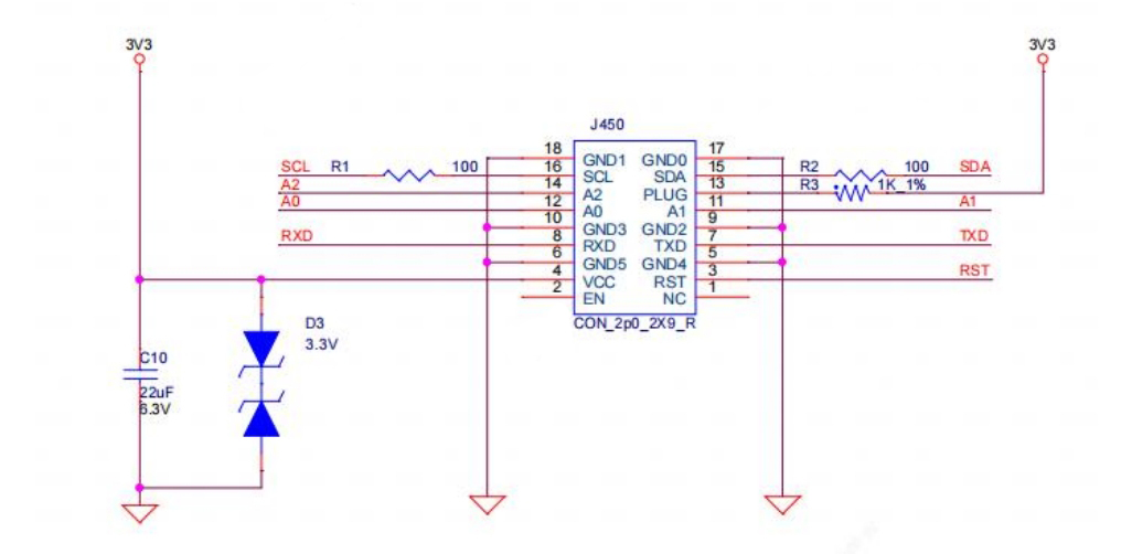
Figure 4-9
6. Overall architecture:
The entire machine primarily consists of 3 hash boards, 1 control board, an APW121215 power supply, and 4 cooling fans (26000 RPM + 27000 RPM), as shown in Figure 4-10.
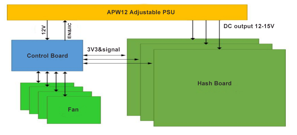
Figure 4-10
V. Common Hash Board Faults and Troubleshooting Steps
1. Symptom: Single board test detects 0 chips (PT1/PT3 station)
Step 1: First, investigate the power supply output.
Step 2: Check the voltage domain output. If there's power supply at 15V, domain voltages are usually present; prioritize measuring the output of the hash board's power terminals.
Step 3: Inspect the boost circuit output; test points C56, 57 should show 19-20V (as shown in Figure 4-8).
Step 4: Verify each group's LDO 1.2V or PLL 0.8V output.
Step 5: Inspect the chip signal outputs (CLK/CI/RI/BO/RST). Refer to the described voltage value ranges for signal directions. If a significant deviation in voltage values is encountered during measurement, compare it with the values measured in adjacent groups to make a determination. (Refer to 5-2)
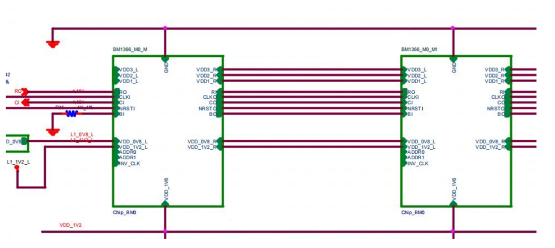
Figure 5-2
2. Symptom: Incomplete chip detection on a single board (PT1/PT3 station)
1) When the LCD displays ASIC NG: (0), first measure the total domain voltage and check if the boost circuit's 20V is normal. Then, use a short circuit probe to short the RX test point between the first and second chips and the 1V2 test point, and run the chip finding program. Observe the serial port log; if it still finds 0 chips, one of the following issues might be present:
a-1) Use a multimeter to measure whether the diode or impedance of the 1V2 and 0.8V LDO on the side is normal. Measure the voltage when powered on to see if it is 1.2V or 0.8V. If not, it could be due to an issue with the 1.2V or 0.8V LDO circuit in that domain, poor soldering of the main chip in that domain, short circuit caused by the 0.8V or 1.2V SMD filtering capacitors, or issues with the LDO circuit's IC such as cold solder joints, false soldering, material damage, chip breakdown, LDO breakdown, etc.
a-2) Check if there is any anomaly in the circuit of U5, such as cold solder joints on resistors.
a-3) Check for any short circuits caused by solder bridging between the BSM heatsink and the surrounding area of the chip.
a-4) Inspect whether the first chip has any unsoldered pins (there have been repair cases where, from the side, the pins seemed soldered, but upon removing the chip, it was found that the pins were not actually soldered at all).
2) If in step a) you find 1 chip, this indicates that the first chip and the preceding circuit are functioning correctly. Proceed in a similar manner to troubleshoot subsequent chips. For example, short the 1V2 test point between the 23rd and 24th chips and the RX test point. If the log finds 23 chips, then there's no issue with the first 23 chips; if it still finds 0 chips, first check if the 1V2 is normal. If 1V2 is normal, the issue lies with the chips after the 23rd. Continue troubleshooting using a binary search method until the faulty chip is identified. Suppose the Nth chip is faulty, then when shorting 1V2 and RX between the N-1 and Nth chips, N-1 chips can be found, but when shorting 1V2 and RX between the N and N+1 chips, not all chips can be found.
3) If the LCD displays ASIC NG: (reporting a specific chip), consider the following two scenarios:
d-1) The first scenario; (usually, the reported chip value does not change with each test). In such cases, proceed with repairs according to the standard method of measuring signal voltages. (It's also possible that there are issues with resistors near the chip, BSM process soldering anomalies, etc.)

Figure 5-3
3. Symptom: Single board Pattern NG, i.e., incomplete nonce data return (PT3 station)
Pattern NG occurs due to significant characteristic differences between one chip and the others. Instances have been found where chips with insufficient solder on the BSM surface or faulty chip bodies just needed replacement. Based on log information, the replacement rules are:
1) Inspect the soldering quality of the BSM heatsink.
2) If the chip's exterior is intact, replace the chip with the lowest response rate in each domain.
3) Swap chips with high response rates with those with low response rates to see if the issue follows the chip. If it does, replace the chip. If not, check if the domain voltage is lower than normal, measure if the chip pad pins' resistance values are standard, and if not, check if adjacent small resistors' resistance values are too high. If high, replacing them should resolve the issue.
PS: It's important to note that both domain and ASIC numbering start from 0.
4. Symptom: B_A X PCS (X chips insufficient response)
Swap these chips with ones from other domains that have higher response rates to see if it makes a difference. If not effective, replacing these chips should suffice.
5. Symptom: Chip testing OK, but PT3 function test serial port does not stop (continuous running)
Repair Method: During PT3 testing, observe the serial port printing log. When the serial port starts continuously running, use a short circuit probe to short RX&1.2V, starting with the first chip. If the serial port stops running after shorting, it indicates that the first chip is OK. Continue this method to find the chip that, when shorted, the continuous running issue persists. Generally, it's caused by a faulty chip, which should be replaced.
PT3 Testing Environment Requirements: The temperature for the PT3 testing environment should be between 20°C and 30°C. If the environmental temperature exceeds 35°C, the software will stop testing. Cooling is necessary during measurement, and the following cooling platform can be used for PT1 measurement cooling, running DEBUG firmware.
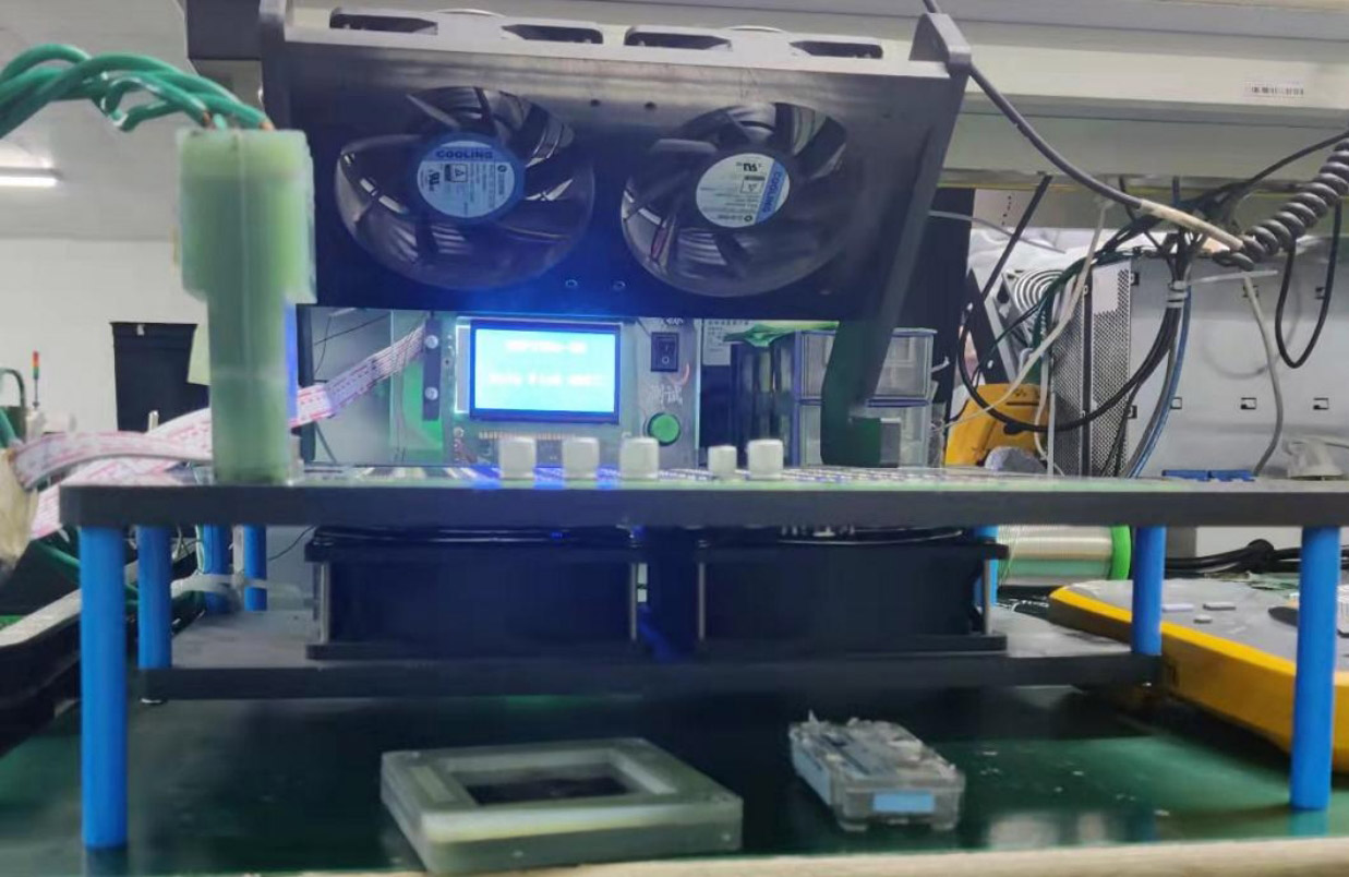
Figure 5-4
6. Chip address error (PT3) repair method: Simply replace the chip that is reporting the error.
7. Single board OK, whole machine hash rate drops
(1) If a chip's RX is returning erratic responses, replace the corresponding faulty chip.
(2) If a domain's LDO power supply is unstable, the resistance value of the resistors in series might be abnormal.
(3) Run low-frequency Debug measurements on the main chip's RI, BI, CLK, etc. signals. If the signal is abnormal after passing through a certain chip, focus on investigating that position. Typically, this indicates soldering issues or a faulty chip.
VI. Control Board Issues Leading to the Following Problems
1. The entire machine does not run
1) Check if the voltage at various output points is normal. For a 3.3V short circuit, first disconnect U8. If the short circuit persists, remove the CPU and measure again. For other abnormal voltages, generally replace the corresponding voltage converter IC.
2) If the voltage is normal, check the soldering condition of DDR/CPU (use X-RAY inspection on the production side).
3) Try updating the flash program with an SD card.
To start the machine normally after flashing the control board with an SD card, the following steps are necessary:
a) After successful flashing, the green LED indicator should remain on; then, power off and restart.
b) After re-powering, wait for 30s (the process of enabling OTP).
c) OTP (One Time Programmable) refers to a type of memory in the MCU, meaning it can be programmed once: after the program is burned into the IC, it cannot be changed or erased again.
Precautions:
(1) If power is suddenly cut off during the OTP process of the 7007 control board, or if less than 30s has elapsed, this can cause the OTP function to fail, preventing the control board from starting (not connecting to the network). In this case, it is necessary to replace U1 (the main control IC FBGA on the control board). The replaced U1 cannot be used in the 19 series again.
(2) U1 from control boards that have had the OTP function enabled cannot be used in other series of machines.
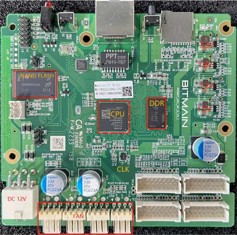
Figure 6-1 (7Z007 control board)
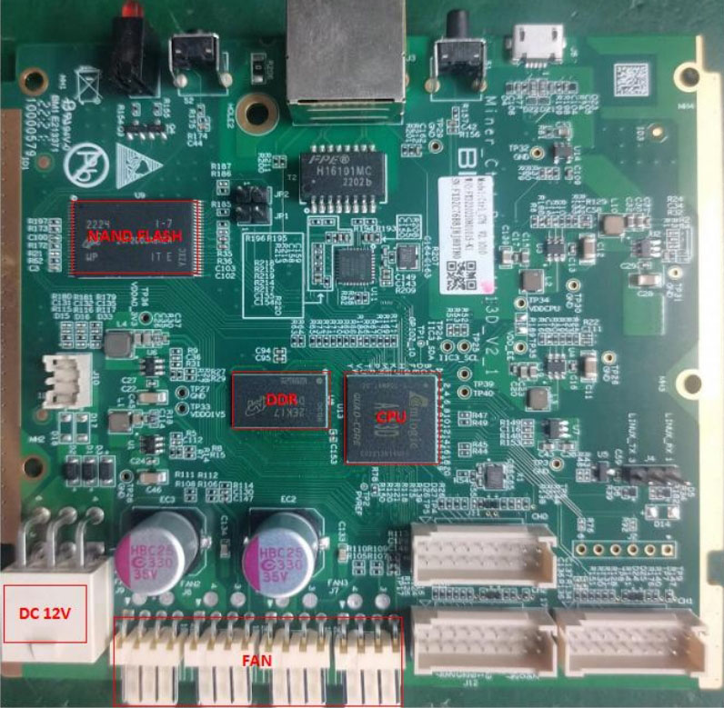
Figure 6-2 (amlogic control board)
2. The entire machine cannot find an IP
The inability to find an IP is likely due to abnormal operation. Refer to point 1 for troubleshooting.
Check the network port, the network transformer T1, and the appearance and soldering condition of the CPU.
3. The entire machine sannot be upgraded
Check the network port, the network transformer T1, and the appearance and soldering condition of the CPU.
4. The entire machine fails to read the hash board or misses connections
A. Check the condition of the ribbon cable connections.
B. Inspect the control board's corresponding chain components.
C. Examine the quality of wave soldering for the row plug pins and the resistance around the plug interface.
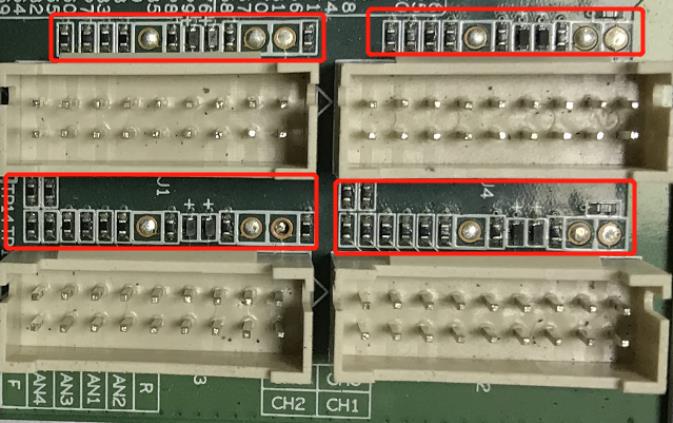
Figure 6-3
VII. Whole Machine Fault Symptoms
1. Initial testing of the whole machine
Refer to the testing process documentation; issues generally arise from assembly process problems or control board process issues.
Common symptoms include inability to detect IP, abnormal fan count detection, and chain detection anomalies. If there are any abnormalities during testing, repair should be conducted based on the monitoring interface and test LOG prompts. The repair methods for initial testing and aging tests are consistent.
2. Aging test: Repair should be based on the monitoring interface during the aging test.
1) Fan display abnormal: Check whether the fan operation is normal, the connection to the control board is secure, and if there are any abnormalities in the control board fan circuit.
2) Missing chain: If only 2 out of 3 hash boards are recognized, there's likely an issue with the connection between the hash board and the control board. Check the ribbon cable for open circuit issues. If the connection is okay, perform PT1/PT3 testing on the single board to see if it passes. If it does, the control board is likely the issue. If the test fails (NG), proceed with repair according to PT1/PT3 methods.
3) Temperature anomaly: First, determine if the issue is caused by high ambient temperature. The monitoring system must ensure PCB temperature does not exceed 75°C and chip temperature does not exceed 95°C. Exceeding these temperatures will trigger an alarm and prevent normal operation. Next, check if fan speed is abnormal as low speed could also cause temperature anomalies. If a specific hash board shows abnormal temperatures, investigate for any issues with the temperature sensors (BHB56902 only has two sensors), referring to single board repair methods.
4) Incomplete chip detection in whole machine: Dismantle and retest with PT1, and repair according to PT1 methods.
5) No hash rate after running for some time, pool connection interrupted: Check the network.
6) Normal conditions during aging test for good machines.
Ⅷ. Other notes
Repair flow chart

Figure 8-1 Repair flowchart
Routine inspection involves several steps to diagnose and repair hash boards:
Visual Inspection: Start with a visual inspection of the hash board to check for PCB deformation, scorch marks, or visible component damage. Address any issues found before proceeding.
Impedance Testing: If the visual inspection reveals no issues, proceed to test the impedance of each voltage domain to detect any short circuits or open circuits. Any issues discovered should be resolved before moving on.
Voltage Testing: Check if each domain's voltage is around 1.15V.
After passing routine checks (especially short circuit tests to prevent damage during power-up), use a test fixture to detect chips and diagnose based on the results.
According to the test fixture display results, start near the faulty chip to measure chip test points (CO/NRST/RX/XIN/BI) and voltages like VDD0V8 and VDD1V2.
Follow signal directions, noting that RX signal travels in reverse (from chip 77 to 1), while signals like CLK, CO, BO, RST travel forward (from 1 to 77), to identify any abnormal fault points.
If a chip is identified as faulty, it may need reflow soldering. Apply flux (preferably no-clean flux) around the chip, heat each solder point until it melts, allowing the chip pins to reflow and solder to the pad. If the issue persists after re-soldering, replace the chip.
After repair, the hash board must pass the test jig inspection twice to be considered good. First, after replacing components and allowing the board to cool, test with the jig. Let it cool again, then perform a second test after the board has completely cooled.
Once a hash board is successfully repaired, maintain detailed repair/analysis records (including date, SN, PCB version, position, fault reason, and responsibility) for feedback to production, after-sales, and R&D.
Finally, reassemble into a complete machine for routine aging tests. Repaired good items should re-enter the production line starting from the first station (at least visual inspection and PT1/PT3 test stations) to ensure quality continuity.
We use cookles to Improve your online experience. By continuing browsing this website, we assume you agree our use of cookies.