


Antminer S21 T21 Hash Board Repair Guide
I. Maintenance platform/tool/equipment preparation requirements
1. Platform requirements:
Anti-static repair workbench (the workbench must be grounded), anti-static wrist strap and grounding.
2. Equipment requirements:
Thermostatic soldering iron (350-380 degrees Celsius), fine-tip soldering iron tip for soldering small SMD resistors and capacitors; hot air gun, BGA rework station for chip/BGA removal and soldering; multimeter, soldering steel needles covered with heat-shrink tubing for easy measurement (Fluke recommended); oscilloscope, ethernet cable (Requirements: for Internet connection, stable network).
3. Repair test tools requirements:
S21 power supply uses APW171215a, 12V-15V, V1.3, safety regulations (calibration). Or use other power supplies in the BOM and power adapter cables (DIY: use thick copper wires for the positive and negative poles to connect the power supply and the hash board. It is recommended to use 4AWG copper wires with a length of less than 60cm, only for PT1 and repair testing) used to power hash boards.
The fixture uses a V2.1 or V2.3 control board (material number ZJ0001000004). The positive and negative poles of the test fixture's power supply need to be installed with discharge resistors. Use cement resistors of 20 ohms and above 100W. When using the 19 series universal test fixture for the first time, need to swipe the fixture B047 version (refer to the S21 test guidance document for details).
T21 PT3 test power supply APW11A1216-1a, 12V-16V, V1.1, safety regulations (calibration), PT1 can use conventional 1215 PSU.
4. Repair auxiliary materials/tools requirements:
Solder paste M705, flux, cleaning solution with anhydrous alcohol (cleaning solution is used to clean flux residues after repair); thermal gel (specification: Fujipoly SPG-30B) used to apply on the chip surface after repair; tin tool stencil (BM1368 LGA 6mm * 8mm chip size), desoldering wire; solder balls (recommended diameter 0.4mm); when replacing a new chip, solder paste must be applied to the chip pins before soldering onto the hash board, apply thermal gel evenly on the chip surface before attaching the large heatsink.
5. Common spare parts for repair:
SMD resistor 33 ohms, ±1%, 1/20W, R0201 (0603);
SMD resistor 10K, ±1%, 1/16W, 0402;
SMD resistor 0 ohms, ±5%, 1/16W, 0402;
SMD ceramic capacitor 1uF, +/-10%, 16V, X5R, 0402;
SMD ceramic capacitor 1uF, 6.3V, 20%, X5R, C0201 (0603);
SMD ceramic capacitor 22uF, +/-20%, 6.3V, X5R, 0603.
II. Repair requirements
1. When replacing chips, pay attention to the operation techniques. After replacing any components, ensure there is no visible deformation of the PCB. Check for missing parts, open circuits, or short circuits around the replaced components.
2. Repair personnel must have certain electronic knowledge, at least one year of repair experience, and be proficient in BGA/QFN/LGA soldering techniques.
3. After repair, the hash board must be tested at least twice with both results being OK to pass. Each work order has a corresponding number of hash board SNs, and each board must be unique. 4. During repair testing, SNs must not be cross-scanned or reused.
Check if the tools and testing fixtures are working properly. Ensure the repair workstation's test software parameters and the version of the test fixture are correct.
5. For testing after replacing chips, first perform a chip detection test. If it passes, proceed with the PT3 sweep function test. Ensure the heatsink assembly is properly installed for functional testing. Apply thermal gel evenly on the chip surface when installing the heatsink, and connect the fan to the test fixture for controlled testing.
6. Without fan cooling or continuous PT1 testing, the chip may overheat and damage the board.
7. When measuring signals and voltages with the heatsink attached, use a fan to blow air on the TOP side for measurement.
8. When replacing a new chip, use a tin stencil to apply solder paste to the chip pins. Ensure the chip is pre-tinned before soldering it onto the PCBA for repair.
9. All fixtures at the repair end must use Test_Mode and scan mode for testing. After the test passes, the production end will start from the first test station, proceed with normal machine assembly and aging (following the same level assembly).
10. After the PCBA with the removed heatsink is repaired and confirmed OK, be sure to reapply thermal paste to the heatsink before reinstallation and flow line testing (otherwise, the whole machine may not operate properly).
III. Test fixture creation and precautions
(The fixture should meet the cooling requirements of the hash board and facilitate signal measurement)
1. Initial use of BHB68XXX series test fixture
Update the fixture control board's FPGA using an SD card with the program. After unzipping, copy it to the SD card and insert the card into the fixture slot. Power it on and wait for about 1 minute until the control board indicator light double blinks 3 times, indicating the update is complete. (If not updated, the test may keep reporting a certain chip as defective).

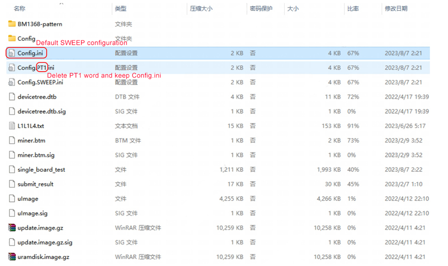
2. Make the test SD card according to the requirements. For PT1 chip detection and PT3 function testing, directly decompress the compressed package to create an SD card. After decompression, delete the original Config file first, such as Config.PT1.ini. The configuration file is named Config.ini, and then click "Yes". The final configuration file is "Config.ini". (The repaired board must be streamlined and tested again from PT1 according to the production process. Maintenance personnel are not allowed to skip the testing pipeline operation without permission)
IV. Principle overview
1. T21 & S21 (BHB68xxx) hash board working structure
The hash board is composed of 108 BM1368 chips (PCB silk screen sequence BM1-BM108), divided into 12 groups (domains), with each domain consisting of 9 ASICs. The working domain voltage for the BM1368 chips used in the BHB68XXX hash board is approximately 1.2V. From domain 1 to domain 10, the VDDIO of the chips is powered by 1.2V & 0.8V LDOs. Each domain uses 3 LDOs (one LDO outputs 1.2V, and two LDOs output 0.8V). The 11th and 12th high-voltage domains each use two MP2019 (U166, U200) to output 2V to supply the LDOs, which then supply VDDIO to the chips. Specifically, LDO U165 and U167 (1.2V & 0.8V) are powered by U166 (MP2019), and the other two LDOs U201 and U199 are powered by U200 (MP2019) with 2V output for their supply, as shown in Figure 4-1.
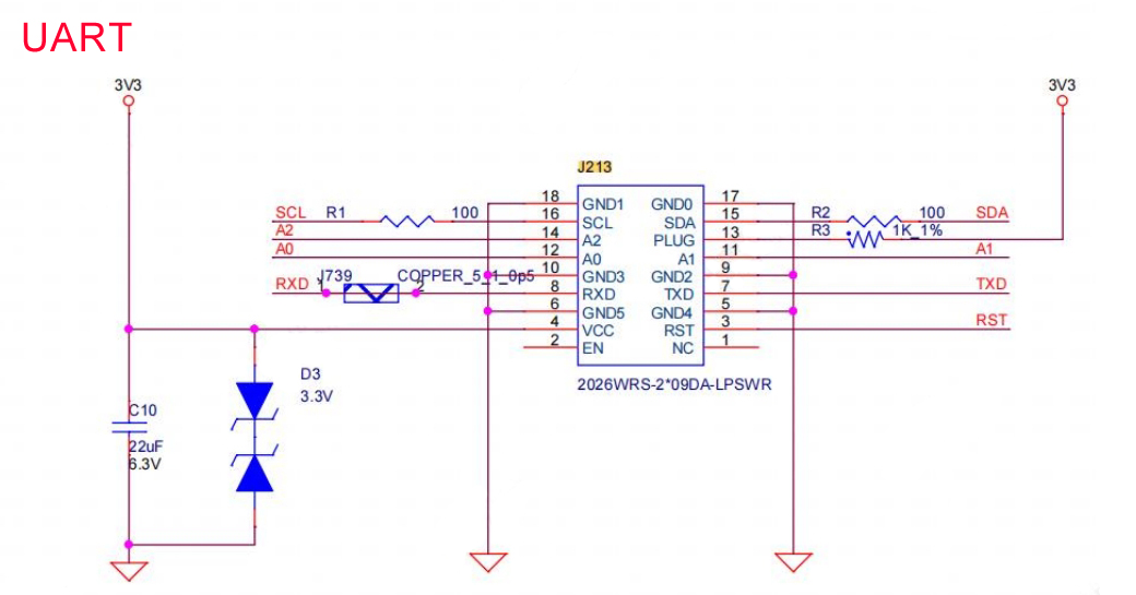
The S21 hash board, compared to the 1366 model, also adds 11 level shifters to perform addition operations on chip-related signals, using a total of 11 level shifters from the second domain to the last domain. As shown in Figure 4-2, the blue box indicates the direction. level_shifter 0 to 9 uses voltage across 5 domains for power supply. For example, level_shifter0 takes the 5th domain voltage for power supply, and so on, which is about 6V. Level shifters 10 and 11 are powered by U118, which outputs VDD_LDO, and U118 input voltage is derived from the boost circuit at 19V, as shown in Figure 4-2. Temperature sensors use 2 pieces of U5 and U7 (T0-T1), one at the inlet and one at the outlet, as shown in Figure 4-3.
Hashboard domain 12 path note: Compared with 1362 and 1398, 1368 cancels the MOS and PIC circuits. Starting from the second domain, 11 operational amplifiers (op amps) were added for signal addition. Generally, if PT1&PT3 is defective at the 2-domain handover position, the op-amp can be checked first, including 12M baud rate detection chip abnormalities, etc. (The chip position in the PT3 test log starts counting from 0, asic 0-107, and the voltage domain also starts counting from 0, that is, domain0-domain11)
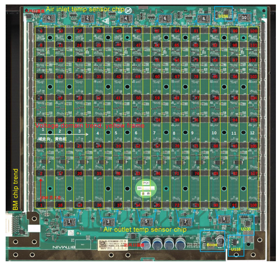
Figure 4-1
BOOST circuit schematic diagram:


Figure 4-2
Temperature sensing circuit schematic diagram:
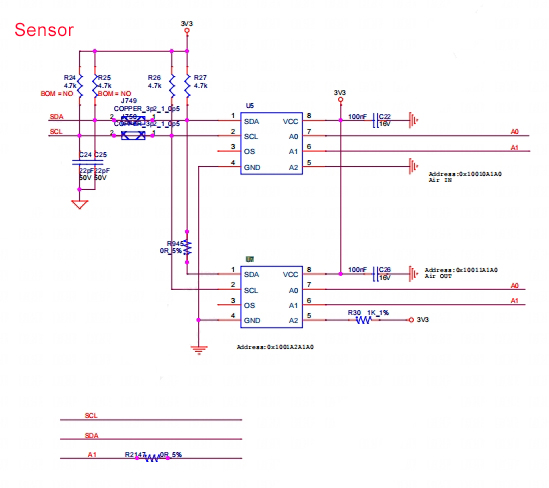
Figure 4-3
2. BHB68XXX hash board boost circuit:
The boost is powered by the power supply and VDD_IN is converted to 25V through U206, as shown in Figure 4-3 and 4-4.
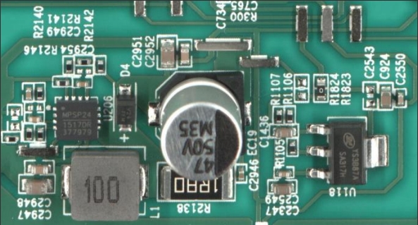
Figure 4-4
3. BHB68XXX chip signal flow:
CLK signal flow: Generated by the Y1 25M crystal oscillator, the CLK signal flows from chip BM1 to chip BM108. The voltage is approximately 0.58 to 0.6V;

TX (CI, CO) signal flow: The TX signal flows from pin 7 (3.3V) of the IO port, through the level-shifting IC U1, and then from chip BM1 to chip BM108. The multimeter measures about 1.1V.
RX (RI, RO) signal flow: The RX signal flows from chip BM108 to chip BM1, through U2, and back to pin 8 of the signal ribbon cable connector, then back to the control board. The multimeter measures about 1.1V.
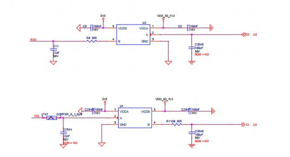
BO (BI, BO) signal flow: The BO signal flows from chip BM1 to chip BM108.
RST signal flow: The RST signal enters from pin 3 of the IO port, passes through R1020, and then flows from chip BM1 to chip BM108. The multimeter measures approximately 1.2V.

4. Whole machine architecture:
The S21 miner is mainly composed of 3 hash boards, 1 control board, and an APW171215a power supply, as shown in Figure 4-5.
The T21 miner is mainly composed of 3 hash boards, 1 control board, and an APW11A1216-1a PSU, see Figure 4-5.
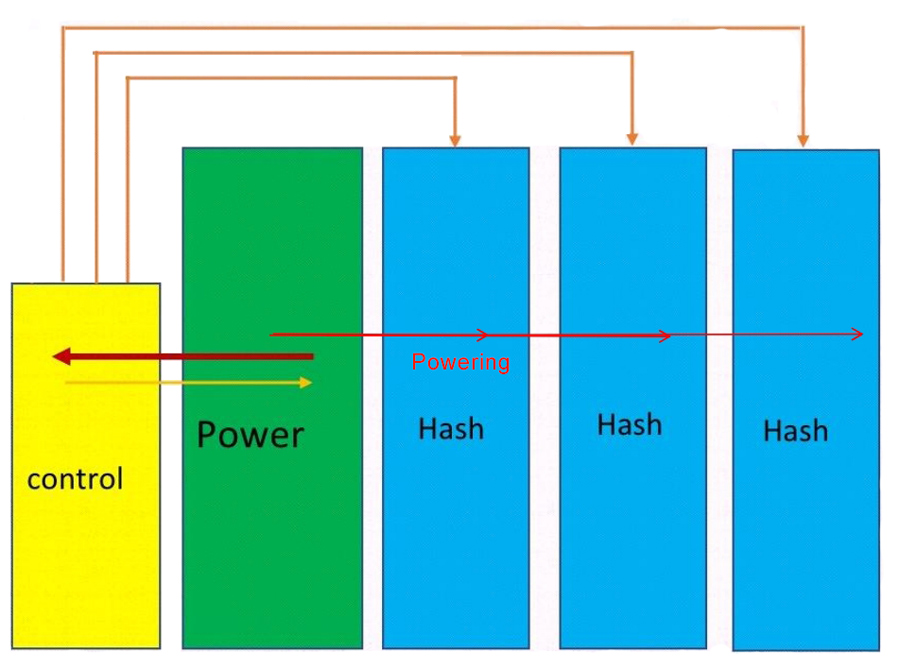
Figure 4-5
V. Common fault phenomena and troubleshooting steps for hash board
1. Phenomenon: single board test detects 0 chips (PT1 station)
1) Troubleshoot the power output. Please check Figure 5-1.
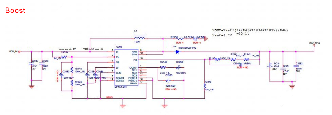
Figure 5-1
2) Check the voltage domain output. Measure if it is approximately 1.1V. If VDD_IN is powered, there should generally be voltage in the domain. Prioritize measuring the output at the hash board power terminal.
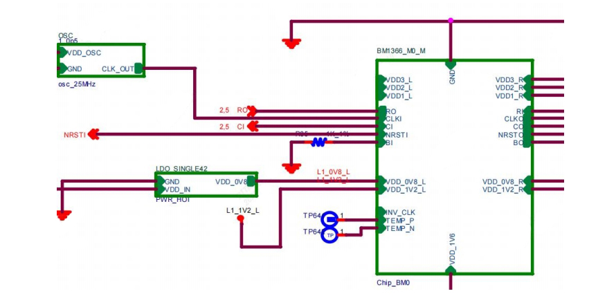
Figure 5-2
3) Check if CLK has output. Measure around BM1. If there is an output, measure the last chip to see if CLK is present. If not, repair it with dichotomy.
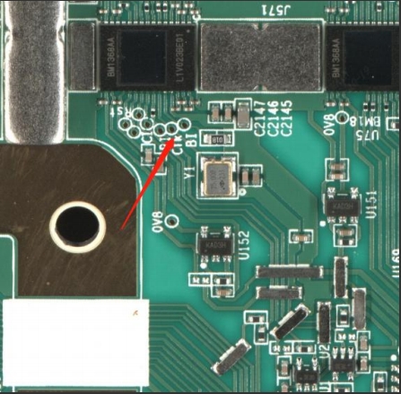
Figure 5-3
4) Check each group of LDO 1.2V or PLL 0.8V output.

Figure 5-4
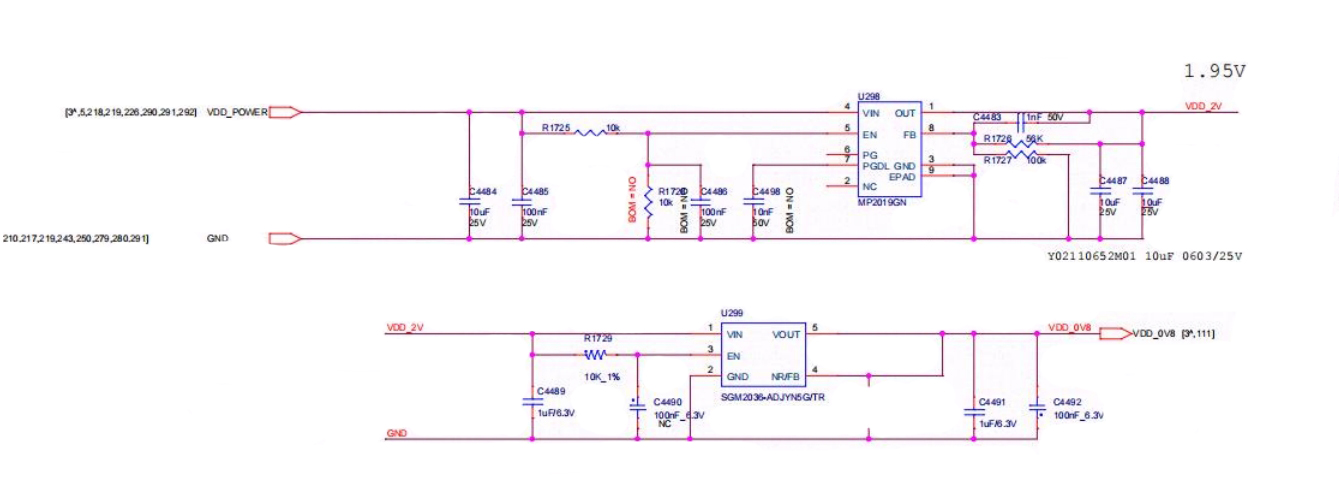
Figure 5-5
5) Check the chip signal outputs (CLK/CI/RI/BO/RST) against the voltage ranges described in the signal flow. If there is a significant voltage deviation, compare it with the measurements from adjacent groups to determine the issue.
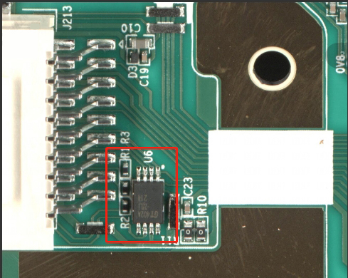
2. When the test fixture LCD displays EEPROM NG
Check if U6 and the surrounding components are soldered correctly. Ensure that the ribbon cable connections are secure and functioning properly.
3. When the test fixture LCD displays Sensor NG
When the test reads abnormal temperatures, follow these steps to troubleshoot:
A) Check the serial log. If sensor=0, inspect the U5 and U7 chips and the adjacent SMD resistors and capacitors to ensure they are soldered correctly.
B) If Sensor={0, 1}, the corresponding sensor positions are {U5, U7}. Refer to Figure 5-6 for the specific locations. Pay special attention to ensuring the 3.3V power supply is normal, which is provided by the control board to J213.
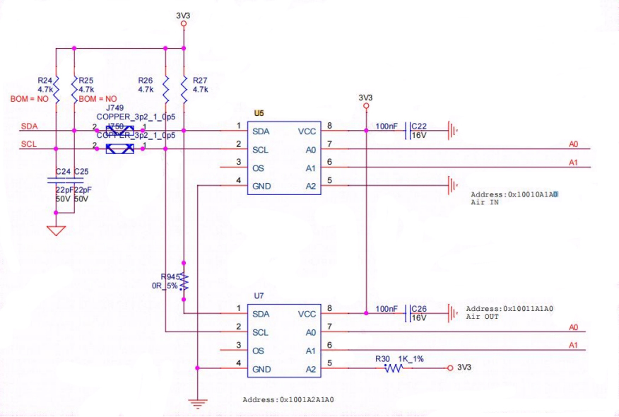
Figure 5-6
4. When the test fixture LCD displays INIT NG TEMP
When the test reads abnormal temperatures at the inlet and outlet, check if U4, U5, and the adjacent SMD resistors and capacitors are soldered correctly.
5. Phenomenon: single board chip detection incomplete (PT1/PT3 (sweep) stations)
a) When the test fixture LCD displays ASIC NG: (0), first measure the total domain voltage (around 15V) and ensure that the voltage in individual domains is normal. Then, use a short circuit probe to short the RO and 1V2 test points between the 1st and 2nd chips, and run the chip detection program. Check the serial log. If 0 chips are still detected, it may be one of the following situations:
a-1) Use a multimeter to measure the voltage at the 1V2 and 0V8 test points. If the voltages are not 1.2V and 0.8V, respectively, there may be an issue with the 1.2V or 0.8V LDO circuit in that domain, or the two ASIC chips in that domain may not be soldered properly. This is often caused by short-circuited 0.8V or 1.2V SMD filter capacitors (measure the resistance of the related SMD filter capacitors on both sides of the PCBA). Alternatively, measure the VDDIO to ground impedance of the chip. If abnormal, disconnect one chip. If the impedance or diode value is still abnormal after disconnecting, remove the corresponding chip.
a-2) Check if the U1 and U2 circuits are abnormal, such as resistors with cold solder joints.
a-3) If the 1V2 and 0V8 voltages are normal, sequentially measure the RO, RST, CLK, CI, and BI signals to ensure they are within normal ranges.
a-4) A 3.3V short circuit, fan malfunction, or cooling issue can cause U5 and U7 to burn out, leading to similar faults. First, measure the impedance of the 3.3V to the ground. If a short circuit is detected, remove the shorted components. Once the impedance returns to normal, reinstall the corresponding components.
b) If in step a), 1 chip is found, it indicates that the first chip and the preceding circuit are OK, and the binary search method can be used for fault localization. For example, short the 1V2 test point and RO test point between the 38th and 39th chips. If the log can find 38 chips, then the first 38 chips are not problematic (if 0 chips are still found, first check whether the 1V2 is normal; usually, the problem lies in the chips after the 38th chip). Continue using the binary search method to locate the faulty chip. (Assume the Nth chip is faulty, short the 1V2 and RO test points between the N-1 and N chips. If N-1 chips are found, but shorting the 1V2 and RO test points between the N and N+1 chips results in 0 chips found, the N chip is faulty).
c) When the test fixture LCD shows ASIC NG: (X, consistently reporting a specific chip), there are 2 scenarios:
c-1) The testing time is approximately the same as for an OK board (usually, the value of X does not change with each test) (the testing time refers to the time from pressing the start test button to the LCD displaying ASIC NG: (X)). This is likely caused by poor soldering of the CLK, CI, and BO resistors before and after the Xth chip, so focus on inspecting these 6 resistors. There is a small probability that it is caused by pin soldering abnormalities in the three chips X-1, X, and X+1.
c-2) The chip's appearance is normal, and the voltage signals are correct, indicating the chip itself is likely defective.
6. Phenomenon: single board Pattern NG, incomplete Nonce data return (PT3 Station)
Pattern NG is caused by significant differences in the characteristics of certain chips compared to others. There are currently several adverse causes:
It is found that the chip die is damaged, so only need to replace the chip;
Chip bridging, virtual soldering (the nonce reply number of two chips in one domain is 0 or 1);
Low domain voltage, 1.2V and 0.8V are normal, the chip itself has problems.
Abnormal nonce returns from multiple chips or the entire domain, measure the domain voltage, and troubleshoot from the domain with the lower voltage.
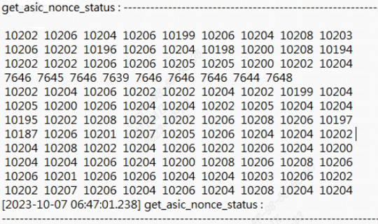
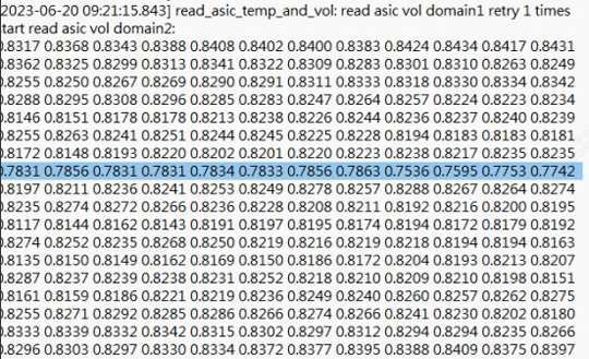
Figure 5-7
PS: It is important to note that the numbers of domain and asic both start from 0;
As shown in Figure 5-10, if the entire domain chip responds abnormally, it is necessary to conduct a preliminary analysis from the test log. The BM1368 series chip supports domain voltage and temperature printing functions (Secure CRT serial port tool. When grabbing the log, please note that the voltage of the ADC printing domain is only about 0.82V. The reason is that one of the small fields cannot be displayed. The theoretical calculation can add about 0.28V).
Next, check the log for abnormal chip temperatures. If one or several chips show abnormally high temperatures, prioritize checking if the heatsink is properly in contact with the chip and if there are any foreign substances on the chip surface. After replacing chips, ensure that any residual flux is thoroughly cleaned off the surface. Residual flux can prevent proper contact with thermal paste, leading to temperature issues. If the heatsink is not the problem, measure the chip's temp_P/N. If abnormalities are found, the chip needs to be replaced.
7. Phenomenon: PT3 Nonce response 0 in the first 6 domains
Repair Method: Inspect the appearance and measure the signal impedance of the chips in the 6 domains. This issue is usually caused by chip short circuits or foreign objects.

8. Phenomenon: During PT3 frequency sweep, the detection chip finds 0 after upscaling
Repair method: Inspect the appearance. During trial production, it is generally found that the issue is caused by chip short circuits, collisions, solder bridges around the resistors near the chips, or the presence of foreign objects.

9. Phenomenon: Whole machine test R:1 error
The log indicates "find x asic" (where x represents a number less than 108), which means that not all hash board chips have been detected. Use PT1 to check for chip abnormalities and perform repairs accordingly. Chain0 represents board 1, Chain2 represents board 3, and the hash board next to the power supply is Chain2 (board 3), while the middle one is Chain1 (board 2).
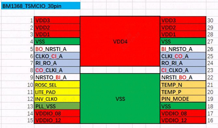
10. When PT1 chip batch abnormalities occur
Refer to the following PIN diagram and use a multimeter in ohm mode to measure the corresponding impedance output.
VI. Control board issues leading to the following problems
1. The whole machine does not operate
Check if the voltage at several output points is normal. If there is a 3.3V short circuit, first disconnect U8. If the short circuit persists, remove the CPU and measure again. For other voltage anomalies, generally replace the corresponding voltage converter IC.
If the voltage is normal, check the soldering conditions of the DDR/CPU (X-RAY inspection at the production end).
Attempt to update the flash program using an SD card.
To properly start a machine with a flashed control board, follow these steps:
a) After the flash is successful, the green LED indicator light is always on. At this time, turn off the power and restart;
b) After repowering, wait for 30 seconds (this is the time required for OTP initialization).
c) OTP (one-time programmable) is a type of memory in the MCU that, once programmed, cannot be changed or cleared.
Precautions:
(1) If the 7007 control board suddenly loses power during the OTP process or the time does not reach 30 seconds, it will cause the control panel to fail to open the OTP function and the control panel will not start (not connect to the Internet). U1 (control board main control IC FBGA) needs to be replaced. The replaced U1 can no longer be used in the 19 series.
(2) For control boards with the OTP function enabled, U1 cannot be used on other series of models.
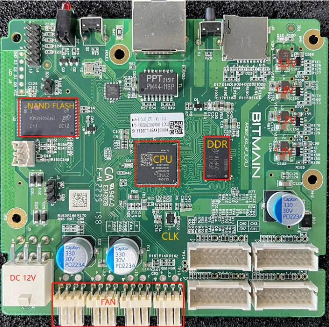
Figure 6-1 (7Z007 control board)
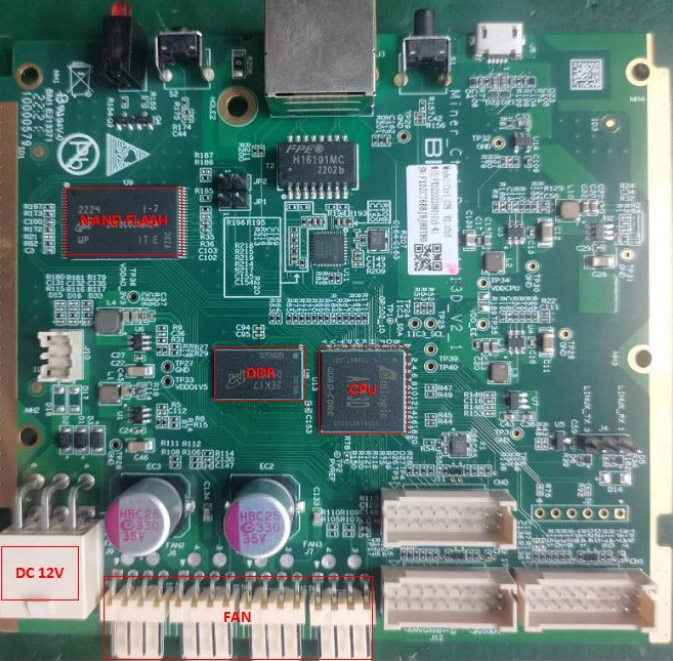
Figure 6-2(amlogic control board)
2. The whole machine cannot find the IP
This issue is most likely caused by an operational anomaly. Refer to point 1 for troubleshooting.
Check the appearance and soldering of the Ethernet port, network transformer T1, and CPU.
3. The whole machine cannot upgrade
Check the appearance and soldering of the Ethernet port, network transformer T1, and CPU.
4. The whole machine fails to read hash boards or missing chains
A. Check the connection status of the ribbon cables.
B. Inspect the control board components corresponding to the chain.
C. Check the wave soldering quality of the pin headers and the resistors around the plug-in interface.
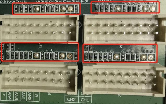
Figure 6-3
VII. Whole machine fault phenomena
(Note that the whole machine is divided into HEM and NEM modes. Please check the log when repairing. It is necessary to determine whether it corresponds to high-frequency or low-frequency NG before repairing.)
1. Initial whole machine test
Referring to the test process document, the general problems are assembly process and control board process problems.
Common phenomena: IP cannot be detected, abnormal number of fans detected, abnormal chain detection. If an abnormality occurs during the test, repairs must be carried out according to the monitoring interface and test LOG prompts. The maintenance methods for the initial test of the whole machine and the aging test are the same.
2. Aging test
1) Fan abnormality: Check whether the fan is working normally, whether the connection of the control board is normal, and whether there is any abnormality in the fan circuit of the control board.
2) Missing chains: If only 2 out of 3 hash boards are recognized, this issue is usually due to a connection problem between the hash boards and the control board. Inspect the ribbon cables for any open circuits. If the connections are OK, individually test the boards using PT1/PT3 to see if they pass. If the boards pass the tests, the issue likely lies with the control board. If the boards fail the tests, repair them according to the PT1/PT3 repair methods.
3) Temperature anomaly: First, check if the ambient temperature is too high. The PCB temperature in the monitoring system should not exceed 75°C, and the chip temperature should not exceed 95°C. If the PCB exceeds 75°C or the chip exceeds 95°C, the machine will alarm and cannot operate normally. Next, check if the fan speed is abnormal; low fan speed can also cause temperature anomalies. If a specific hash board has an abnormal temperature, check the temperature sensors on the hash board (BHB56902 has only two temperature sensors) and refer to single-board repair methods.
4) Incomplete chip detection on the whole machine: Disassemble the single board and retest with PT1. Repair according to the PT1 repair methods.
5) No hash rate after running for a while, mining pool connection interrupted: Check the network.
6) Refer to the aging test status of normal good machines and defective machines as shown in Figure 7-1.
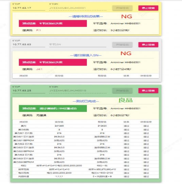
Figure 7-1
Aging test: During aging tests, repairs should be based on the monitoring interface tests, such as:
1) Missing chains: Missing chains mean that 3 boards are present but 1 board is missing. This is usually due to a connection issue between the hash boards and the control board. Inspect the ribbon cables for any open circuits. If the connections are OK, test the single board with PT3. If it passes, the issue is likely with the control board. If it does not pass, repair the board using PT3 repair methods.
2) Temperature anomaly: This is usually caused by high temperatures. The monitoring system specifies that the maximum PCB temperature should not exceed 80°C and the chip temperature should not exceed 95°C. If these temperatures are exceeded, the machine will alarm and stop working. Generally, check if the exhaust temperature exceeds 45°C and inspect the thermal gel, as it can also cause temperature anomalies.
3) Incomplete chip detection: If the OM firmware can boot and run while the IM firmware cannot, and the OM firmware hash rate is 2/3 or 1/3 of the normal value, check the log for insufficient chip numbers. If the chip count is insufficient, refer to PT1 & PT3 testing and repair methods.
4) No hash rate after running for a while, mining pool connection interrupted: Check the network.
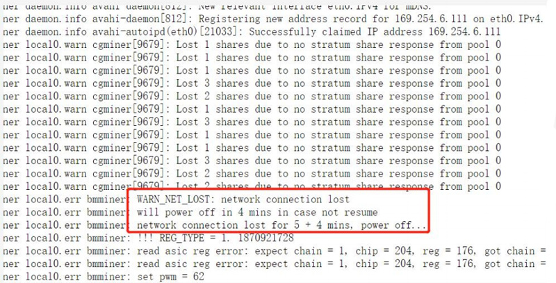
5) Aging test status of normal products:
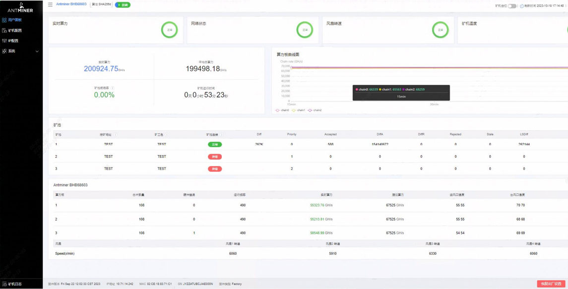
6) The whole machine loses hash rate JX:1:
First, check the machine operation page and the whole machine log to see if any chips are marked with a red X. If it is determined that one or multiple chips are affected, read the chip temperature and domain voltage through the 6060 port after the webpage IP to determine if there are any abnormalities. If the temperature at the X-marked chip location is abnormal, prioritize checking the cooling system. If the domain voltage is abnormal, measure the related chip impedance for any irregularities.
If both chip temperature and domain voltage are normal, but one of the boards reports multiple bad ASICs, and the issue cannot be repaired, validate by retesting with PT3. If the test is OK, collect the data and report it to quality engineering for further analysis.
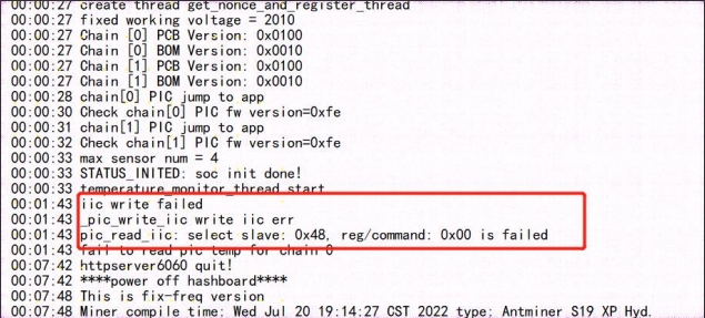
7) The whole machine runs I2C error. It is usually a problem of cable contact. To resolve the issue, restart or re-plug the cable.
3. After-sales repair and production maintenance PT1 test platform construction (the test requires fans to blow up and down for heat dissipation).
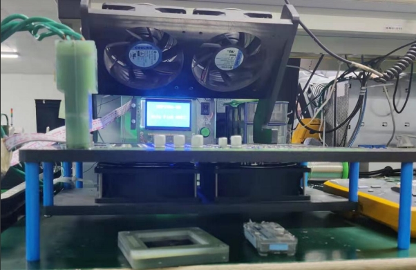
Figure 7-4
After the repair, use the scan mode to test PT1 before testing PT3.
VIII. Other precautions
Repair flowchart

Figure 8-1 Repair flowchart
General inspection: First, perform a visual inspection of the hash board to be repaired. Observe whether the PCB is deformed or scorched. If there is any problem, it must be dealt with first. Whether there are obvious signs of burnt parts, offset parts due to impact or missing parts, etc. Secondly, if there is no problem after visual inspection, the impedance of each voltage domain can be detected first. Check for short or open circuit conditions. If found, it must be dealt with first. Again, check whether the voltage of each domain is about 1.2V.
After there are no problems in the routine inspection (short circuit detection in routine testing is generally necessary to avoid burning the chip or other materials due to short circuit when power is on), the test fixture can be used to detect the chip, and the positioning judgment can be made based on the test fixture detection results.
According to the display results of the test fixture detection, start from the vicinity of the faulty chip and detect the chip test points (CI/RST/RO/CLK/BI) and VDD0V8, VDD1V2 and other voltages.
According to the signal flow direction, except for the RO signal which is transmitted in the reverse direction (chip No. 108 to No. 1), several of the signals CLK CI BI RST are transmitted in the forward direction (1-108), and the abnormal fault point is found through the power supply sequence.
When locating the faulty chip, the chip needs to be soldered again. The method is to add flux (preferably no-clean flux) around the chip, and then heat the solder joints of the chip pins until they are dissolved. As a result, the chip pins and pads are re-fitted and tinned to achieve the re-tinning effect. If the fault remains the same after re-soldering, the chip can be replaced directly.
After the repair, the hash board must be passed through the test fixture for more than two times before it can be judged as a good product. For the first time, after replacing the accessories, wait for the hash board to cool down, use the test jig to test the pass, and then set it aside to cool down. The second time, wait a few minutes for the hash plate to cool completely before testing again.
After hash board repair OK. Relevant maintenance/analysis records need to be kept.
After recording, install the complete machine for routine aging.
Good products that have been repaired at the production end must be streamlined from the first station of production (at least appearance inspection and PT1/PT3 testing stations).
For defective hash boards that have been repaired, the heat sink thermal grease must be reprinted (otherwise it will cause abnormal heat dissipation and temperature difference).