


Antminer E9pro E11 Hash Board Repair Guide
Ⅰ. Maintenance platform/tools/equipment preparation requirements:
1. Platform requirements:
Anti-static repair workbench (the workbench must be grounded), maintenance personnel must wear anti-static wrist straps.
2. Equipment requirements:
(1) Constant temperature soldering iron (350-380 degrees) and pointed soldering iron tip: used for soldering small components such as chip resistors or capacitors;
(2) Hot air gun, BGA rework station: used for chip / BGA disassembly and soldering (BGA soldering station should be able to solder PCBA larger than 286mm*427mm);
(3) Multimeter: add soldering steel needle and put on heat shrink tubing for easy measurement (Fluke is recommended);
(4) Oscilloscope: It is recommended to use UTD2102CEX+ oscilloscope;
(5) Network cable: connected to the Internet, and the network is stable).
3. Test tool requirements:
(1) APW12 power supply (AP12_12V-15V_V1.2) and power adapter cable: used to power the hash board.
Self-made: Use thick copper wire to connect the PSU and the hash board at the positive and negative poles of the power supply. It is recommended to use 4AWG copper wire with a length of less than 60cm. It is only used for maintenance and testing;
(2) V2.1 control board test fixture (material number: Z11010503): The positive and negative poles of the test fixture's powering need to be equipped with discharge resistors. It is recommended to use 20-50 ohm, 100W or more cement resistors.
4. Maintenance auxiliary materials/tools required:
(1) Solder paste M705, flux;
(2) Board cleaning water and anhydrous alcohol: used to clean the flux residue after maintenance;
(3) Thermal conductive gel (specification: Fujipoly SPG-30B): used to apply on the chip surface after repair;
(4) Tin planting steel mesh, solder wick, solder ball (ball diameter recommended 0.5mm): When replacing a new chip, it needs to be planted in the tin and then soldered to the hash board. The chip surface should be evenly coated with thermal conductive gel and then locked with the heat sink.
(5) Barcode scanner
(6) RS232/TTL adapter board 3.3V
(7) Homemade short-circuit probe: Use pins and cable for soldering, and add the heat shrink sleeve to prevent the probe and the small heat sink from short-circuiting;
5. Common maintenance spare material requirements:
0402 resistors: 0R, 51R, 10K, 4.7K
0402 capacitors: 0.1uf, 1uf
Ⅱ. Maintenance requirements:
1. Pay attention to the operation method when replacing the chip. After replacing any accessories, the PCB board has no obvious deformation. Check whether there are missing parts, open circuits and short circuits in the replaced parts and the surrounding areas.
2. The maintenance personnel must have certain electronic knowledge, more than one year of maintenance experience, and be proficient in BGA/QFN/LGA package welding technology.
3. After the maintenance, the hash board must be tested more than twice to ensure everything is OK before it can pass.
4. Check whether the repair tools and test fixture can work properly, determine the maintenance station test software parameters, test fixture version, etc.
5. When testing the replacement chips, we need to first check whether the capacitor on the back of the chip is short-circuited. After passing, do the functional test. The functional test must ensure that the heat sink is installed in place (each thermal adhesive must be evenly applied before installing the heatsink) and that the cooling fan is at full speed. When using the chassis for heat dissipation, put in one hash board simultaneously to form an air duct.
6. When measuring the signal, assist 4 fans in dissipating heat and maintaining full speed.
7. When powering the hash board, the PSU's negative copper cable must be connected first, then the positive copper cable, and finally the signal cable. When disassembling, the order must be opposite to the installation order. First, remove the signal cable, then the PSU's positive copper cable, and finally, the negative copper cable. If this order is not followed, it is very easy to cause damage to the PIC circuit (not all chips can be found). Before testing PT2, the repaired hash board must be cooled down before testing otherwise, it will cause a test PNG.
8. When replacing a new chip, we need to print the pins and solder paste to ensure that the chip is pre-tinned before soldering it to the PCBA for repair.
9. The test fixtures on the maintenance side all use the Test_Mode mode and the code scanning mode for testing. After the test passes, the production side flows from the first test station and is installed and aged normally (installed at the same level). The test configuration file can be obtained by consulting TE.
Ⅲ. Test fixture production and precautions
The test fixture should meet the requirements of heat dissipation of the hash board and facilitate signal measurement
1. Get the BEE series (E9, E11) test file and hash board PCBA test fixture (material number: Z11010503). The test file name and indicator light are as follows:


Make the test SD card according to needs, and directly decompress the compressed package to make the SD card.
IV. Principle Overview
1. E9 pro and E11 hash board working structure
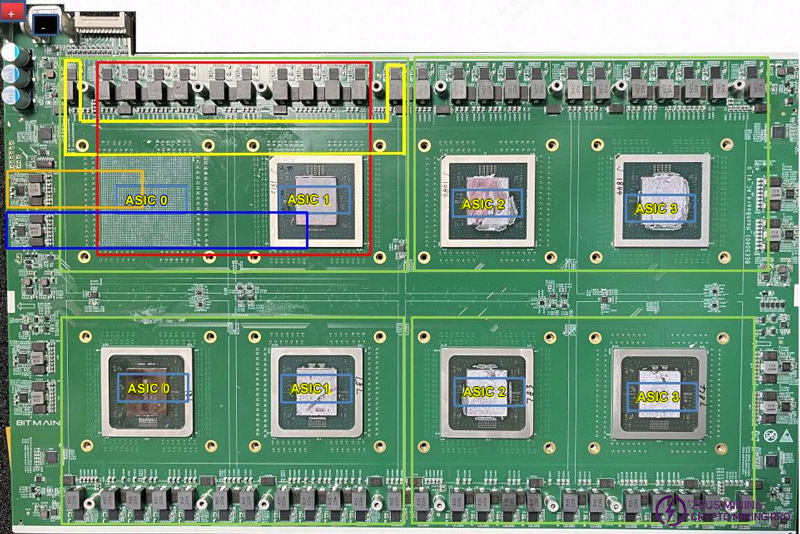
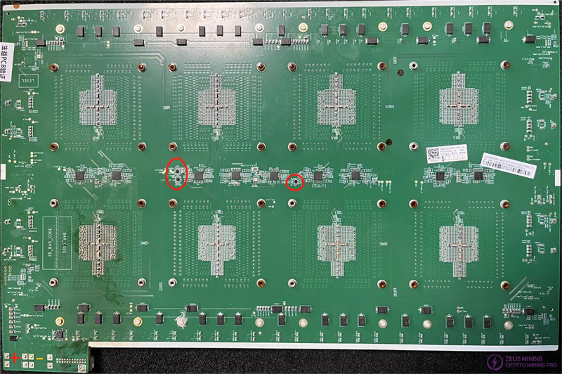
The hash board is composed of 8 BM2280 50*50 BGA chips. Every two chips share a set of power management chips. The red one is VCORE, the yellow one is VP, then the orange and blue ones are VPH.
2. Powering process
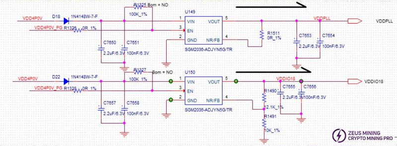
Each two chips share a multi-phase powering set, providing two voltages: VCORE 0.7V and VP 0.9V). The DC-DC circuits on both sides provide VPH 1.2V, and the LDO chip provides VDDIO 1.8V and VDDPLL 0.8V.
In addition, two DC-DCs and lower-level LDOs provide power to the clock chip, clock buffer, and MOS chip, respectively.
3. Low-speed signal flow
(1) CLK (XIN) signal flow, generated by Y2 crystal oscillator, voltage is about 1.8V;
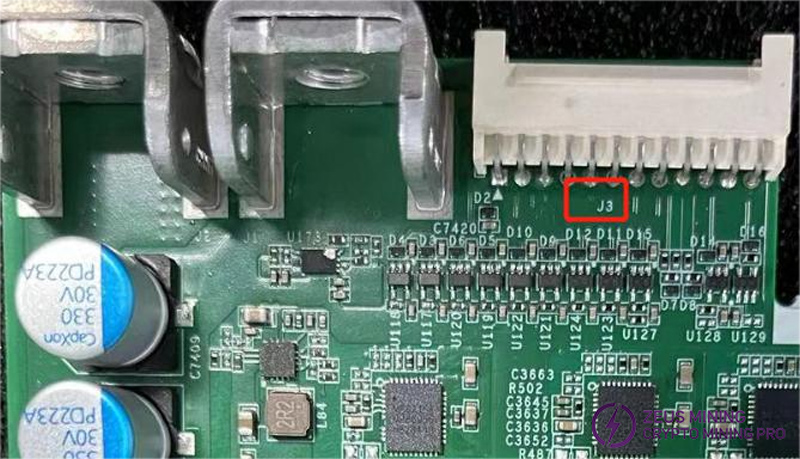
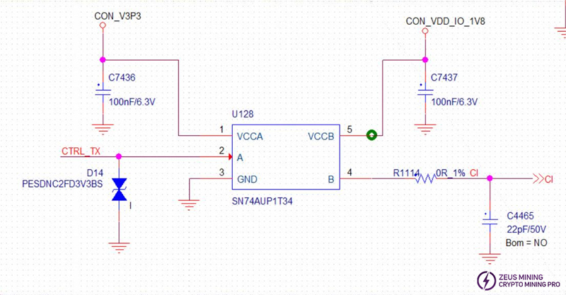
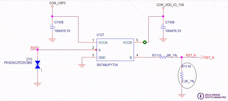
(2) RST and CI signal flow, enter from J3 IO interface pin 15 and pin 22 (3.3V), after conversion by level conversion IC, then transmitted from chip 0 to chip 7; when no IO cable is plugged in, the voltage is 0V, and the test report is 0;
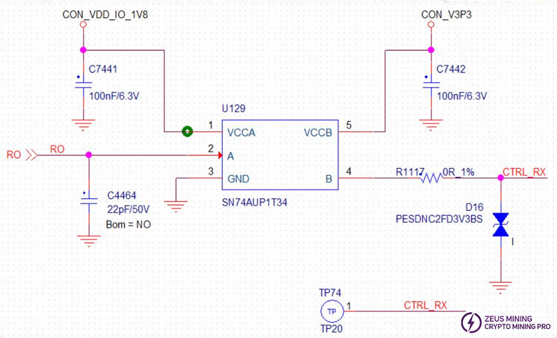
(3) RX (RI, RO) signal flow, from chip 7 to chip 0, through U129 back to the signal cable terminal pin 21, and finally back to the control board; when no IO cable is plugged in, the voltage is 0.3V, but the voltage is 1.8V during operation;
(4) BO (BI, BO) signal flow, from chip 0 to chip 7, the multimeter measured 0V.

4. High-speed serial port signal direction
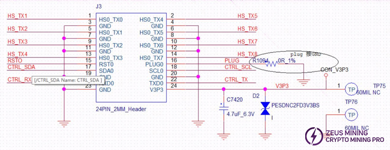
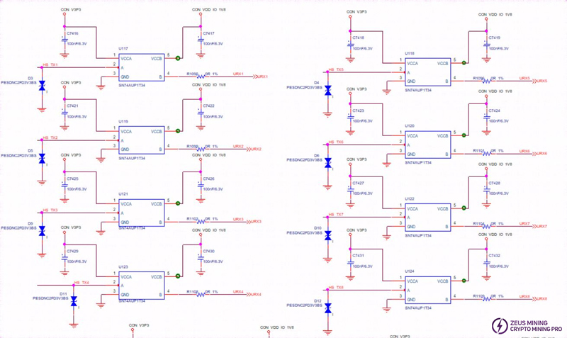
HS_TX1 and HS_TX8 convert the high-speed serial port signal's voltage into 1.8V through the level conversion chip and then connect it to each main chip.

5. Crystal oscillator clock description:
In addition to the Y2 crystal oscillator used to transmit low-speed serial port signals, the E9 pro hash board also has a 100MHz clock for high-speed serdes signals.
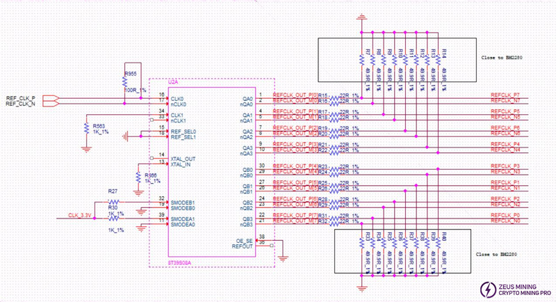
The clock architecture of the E9 pro hash board: After U140 outputs 100MHz, it is divided into 8 paths through U42 and enters U2, U5, U8, U11, U14, U17, U20, and U23, respectively. Then, each chip is divided into 8 paths and outputs to the main chip.

VI. Overall architecture
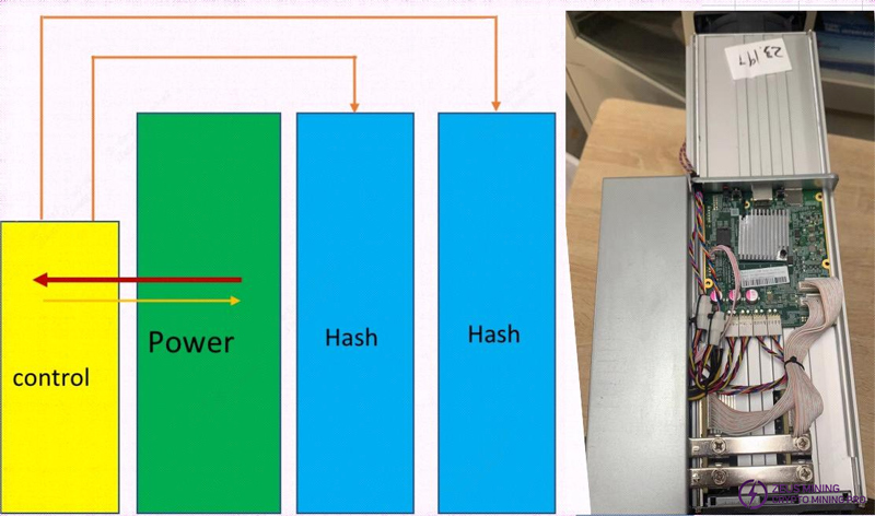
The overall miner consists of 2 hash boards, 1 control board, an APW12 power supply, and 4 cooling fans.
Ⅴ. Common bad phenomena of hash board and troubleshooting steps
1. Phenomenon: Single board test detection chip is 0 (PT2 station)
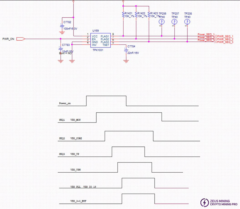
Step 1: Check the power output. Please check whether the voltage of all test points is normal, especially VDDIO1.8V and VDDPLL 0.8V; if the total voltage is normal but there is no LDO powering, check whether the corresponding powering is enabled, and locate it from front to back according to the timing sequence in the figure below.
Step 2: Check the PIC circuit
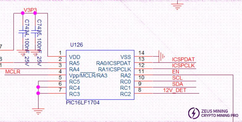
Measure whether there is output at pin 11 of U126; the voltage is about 3.3V. If yes, please continue troubleshooting the problem; if there is no 3.3V, please check the cable connection status of the test fixture and hash board. If OK, re-flash the PIC.
Step 3: Check if the signal cable connection is normal
Start from the beginning of the signal connection to check if there is a signal at CTRL_TX, CTRL_RX, RSTO, etc., and continue to troubleshoot.

2. Phenomenon: No hash rate or low hash rate
(1) First, check the log to see if there are obvious alarms. If there are alarms, locate them according to the alarm instructions;
(2) Check whether the chip's VCORE, VP, and VPH powering are normal. If they are abnormal, first determine the powering problem;
(3) Check whether the 100M clock of the chip exists. If not, check the corresponding chip;
(4) Check whether the 0201 capacitors around the chip have collisions or poor soldering. If so, fill them up.
3. Phenomenon: The rejection rate of the mining pool is high
Step 1: Check whether the connector soldering is intact;

Step 2: Check whether the HS_TX level conversion circuit is normal;
Step 3: Re-flash the firmware or change the mining pool and retest.
VI. PIC burning steps
1. Hash board PIC burning program, download the flashing tool: MPS, Server telecom Core Power Monitor Programming
2. Burning steps:
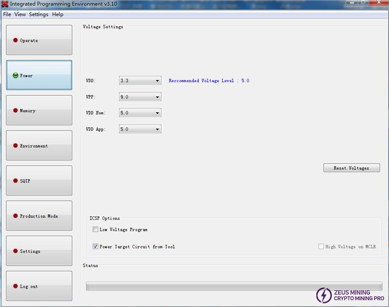
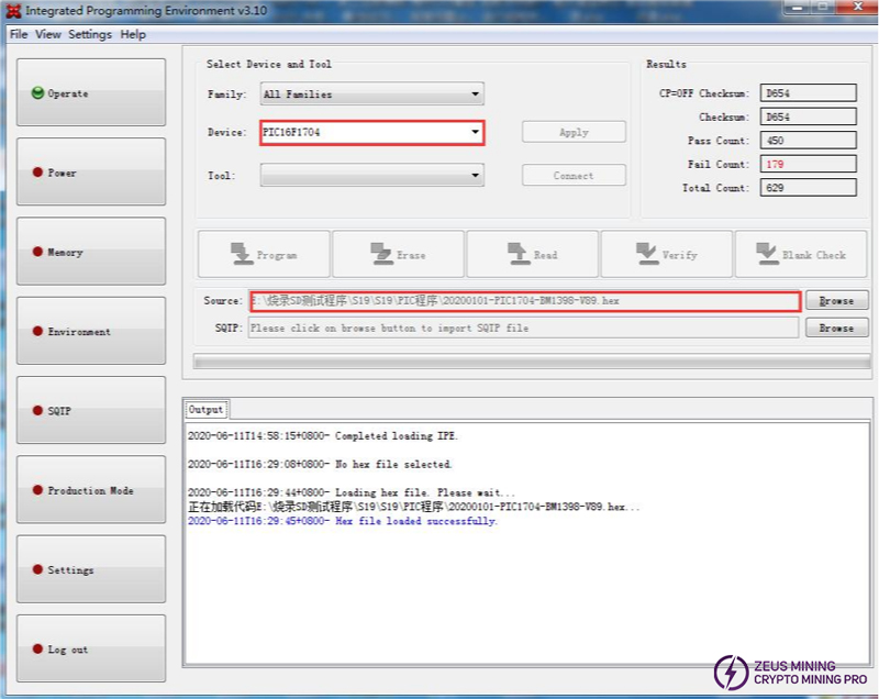
(1) Open MPLAB IPE, select device: PIC16F1704, click Power to select the powering mode, and then click operate.
(2) Select file to find the .HEX file to be flashed.
(3) Click Connect to connect normally.
(4) Click the Program button, and after completion, click Verify, and the prompt verification is completed to prove that the burning is successful.
VII. Failure caused by abnormal control board
1. The whole miner does not run
(1) Check whether the voltage of several voltage output points is normal. If any voltage is short-circuited, disconnect it first; if it is still short-circuited, unplug the corresponding load and measure it. For other voltage abnormalities, generally replace the corresponding voltage conversion IC.
(2) If the voltage is normal, please check the soldering condition of DDR/CPU (X-RAY inspection at the production end)
(3) Try to update the flash program with an SD card;
2. The whole miner cannot find the IP
(1) It is likely that the operation abnormality causes the IP to be found. Refer to point 1 for troubleshooting.
(2) Check the appearance and soldering condition of the network port, network transformer T1, and CPU.
3. The whole miner cannot be upgraded
(1) Check the appearance and soldering condition of the network port, network transformer T1, and CPU.
4. The whole miner fails to read the hash board or the chain is missing
A. Check the cable connection condition.
B. Check the parts of the corresponding chain of the control board.
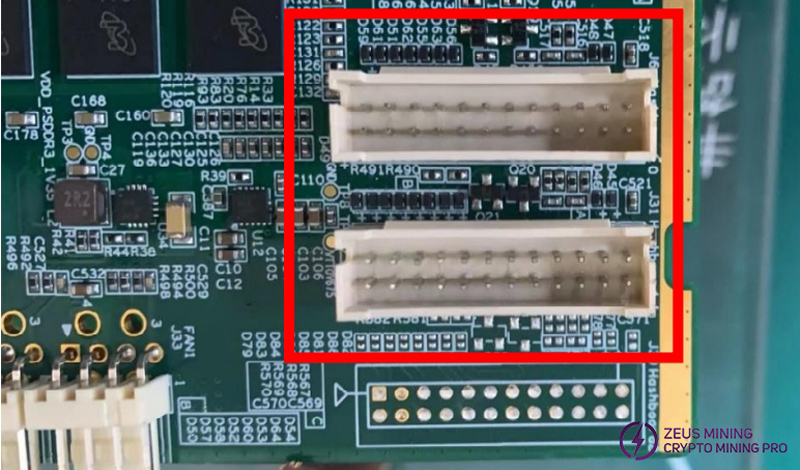
C. Check the wave soldering quality of the socket pins and the resistance around the plug-in interface.
VIII. Whole machine failure phenomenon
1. Whole machine initial test
Refer to the test process file, generally there are assembly process problems and control board process problems.
Common phenomena: IP cannot be detected, abnormal number of detected fans, abnormal chain detection. If an abnormality occurs during the test, repair should be carried out according to the monitoring interface and test LOG prompts. The maintenance methods of the whole machine initial test and aging test are the same.
2. Aging test: During the aging test, repair should be carried out according to the monitoring interface test, for example:
(1) Fan display abnormality: We need to check whether the fan is working normally, whether the connection with the control board is normal, and whether the control board is abnormal.
(2) Missing chain: Missing chain means that 1 of the 2 boards is missing. In most cases, there is a problem with the connection between the hash board and the control board. Check the cable to see if there is an open circuit. If the connection is OK, the single board can be tested with PT2 to see if it can pass the test. If it can pass the test, it can basically be determined that it is a problem with the control board. If it fails the test, use the repair method of repairing PT2 for repair.
(3) Temperature abnormality: Generally, the temperature is high. Our monitoring system sets the maximum PCB temperature to no more than 80 degrees. If it exceeds 80 degrees, the machine will alarm and cannot work normally. Generally, it is caused by the ambient temperature being too high. Abnormal fan operation can also cause temperature abnormality.

(4) No hash rate after running for a period of time: The mining pool connection is interrupted. Check the network.