


Antminer S21 Hydro Hash Board Repair Guide
I. Preparation of repair platform/tools/equipment
1. Platform requirements:
Static electricity repair workbench (workbench must be grounded), anti-static wrist strap and grounding.
2. Equipment requirements:
Constant temperature soldering iron (350℃-380℃), fine tip soldering iron for soldering small SMD resistors and capacitors;
Hot air gun: temperature 350±10℃;
Multimeter, with welded steel needles and heat shrink tubing for easy measurement (Fluke recommended);
Oscilloscope and Ethernet cable (requirements: connect to Internet, stable network).
3. Repair and testing tools requirements:
(1) APW11 power supply, test SWEEP must use APW111721 power calibrated PSU (non-conventional power supply).
DIY power adapter cable: positive and negative poles use thick copper wire to connect the PSU to the hash board. Recommend using 4AWG copper wire, length within 60cm for powering hash board (production testing is carried out using locked copper bars);
(2) Use 19 series universal test fixture, tester bottom package B047 version (part number: ZJ0001000004).
(3) PT1 test supports APW9, APW9+, APW11 PSU.
4. Repair auxiliary materials / tools requirements:
Solder paste M705, flux, circuit board cleaner mixed with anhydrous alcohol, for cleaning flux residues after repair;
Thermal grease (specification: Fujipoly SPG-30B) for application on the chip surface after repair;
Planting tin stencil (6mm * 8mm chip size), desoldering wire: when replacing a new chip, the chip pins need to be tinned and then soldered to the hash board. The chip surface should be evenly coated with thermal conductive gel before installing the water-cooled heat sink.
5. Common spare materials:
SMD resistor 33 ohm, 1%, 1/20W, R0201 (0603);
SMD resistor 10K, ±1%, 1/16W, 0402;
SMD resistor 0 ohm, 1/16W 0402 5%;
SMD ceramic capacitor 1uF, ±10%, 16V, X5R, 0402;
SMD ceramic capacitor 1uF, 6.3V, 20%, X5R, C0201 (0603);
SMD ceramic capacitor 22uF, ±20%, 6.3V, X5R, 0603.
II. Repair requirements
1. Pay attention to the operation method when replacing the chip. After replacing any accessories, there is no obvious deformation of the PCB board. Check whether the replaced parts and the surrounding areas are missing parts, open circuits, or short circuits.
2. Repair personnel must possess adequate electronics knowledge, have over a year of repair experience, and be proficient in soldering BGA/QFN/LGA packages.
3. After repair, the hash board must be tested more than twice and must pass as OK before approval. Each work order corresponds to a specific number of hash board serial numbers (SN), with each board having a unique SN. During test scanning, SN must not be reused.
4. Check that tools and test fixtures are working properly, and ensure that the repair station's testing software parameters and test fixture versions are correct.
5. To test the chip after repair and replacement, it is necessary to first detect the chip and then do the functional test after passing. The functional tests must ensure the water-cooling plate assembly is OK. When installing the water-cooling plate, evenly apply thermal grease on the chip surface, and ensure that the cooling fan is at full speed or connected to a water-cooling radiator device. When using a water-cooling radiator for cooling, a water pump must be added at the water inlet to increase water flow speed (factory tests use PT1).
Note: Testing PT1 without a radiator will cause the chip to overheat and burn the board (must be noted).
6. When testing the PT1 chip and measuring the signal, the heat sink must be installed, otherwise the board will burn out. PT3 tests must connect to an external water cooling radiator, and the water flow rate must be 3-3.5L/min before the test can be performed. The water temperature must be between 32-35℃. If the water temperature is lower or higher than this, the test cannot be performed.
7. When connecting the heat sink to measure the signal and voltage, the measurement can be performed on the BOT surface. The bottom bracket has reserved openings to facilitate the measurement of the signal and voltage point.
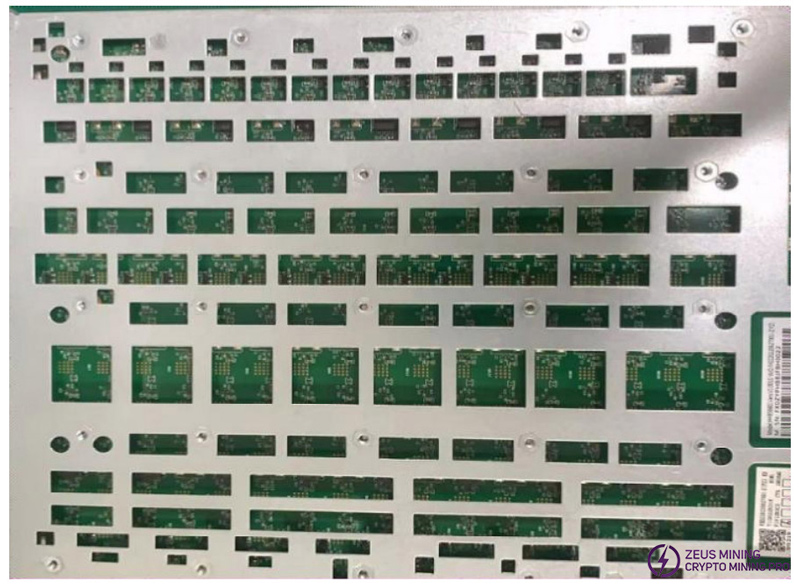
8. When replacing a new chip, print the pins and apply solder paste to ensure the chip is pre-tinned before soldering it to the PCBA for repair.
9. Repair team test fixture should use Test_Mode and scan mode for testing. After passing the test, the production team starts from the first station of the test assembly line and proceeds with normal aging assembly (assembled at the same level).
10. After the PCBA with the heat sink removed has been repaired, the water-cooled heat sink must be re-printed with silicone grease before installation and streamlined testing, otherwise it will cause the whole machine to run poorly.
III. Test fixture fabrication and precautions
(The test fixture should meet the requirements for heat dissipation of the hydro hash board and facilitate signal measurement)
1. Part retrieval number: ZJ0001000004 test fixture; card flash corresponds to the test fixture bottom package.
2. When using the S21 Hyd. series tester for the first time, use the SD card to update the FPGA of the test fixture control board. Unzip and copy the test file to the SD card, and insert it into the test fixture card slot; power on for about 1 minute and wait for the control board's indicator light to double flash three times to complete the update; (If not updated, a chip may continue to report errors during the test).

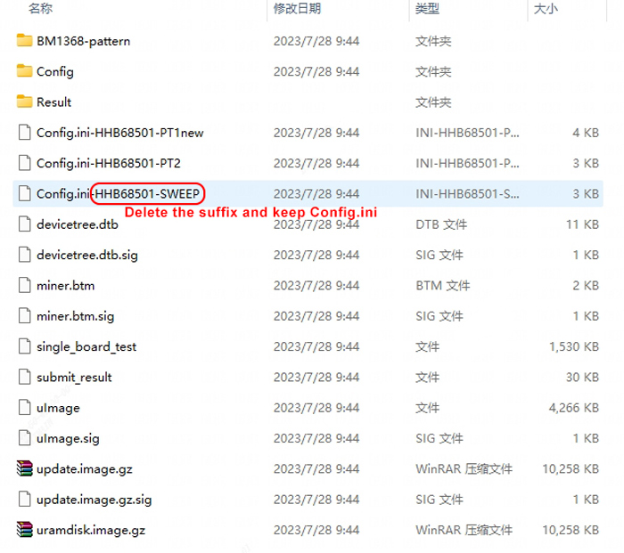
3. Make the test SD card according to the requirements. For PT1 chip inspection and PT3 functional testing, directly unzip the compressed file to make the SD card. After unzipping, first delete the original Config file, such as renaming the Config.ini-HHB68501-SWEEP configuration file to Config.ini, then click "Yes," and the final configuration file will be "Config.ini". (Repaired hash boards must follow the production process to be tested again from PT1 in the test streamline, and repair personnel must not skip the test streamline operation privately.)
4. During PT1 chip testing, the production side, after-sales service side, and outsourced repair side need to be equipped with barcode scanners, serial port tools, and Ethernet cables.
IV. Principle overview
1. S21 Hyd. (HHB68xxx) hash board working structure:
The hash board is composed of 216 BM1368 chips (PCB silk screen order BM1 - BM216), divided into 18 domains, each domain consisting of 12 ASIC chips.
The BM1368 chip used by the S21 hydro hash board has a working domain voltage of about 1.1V.
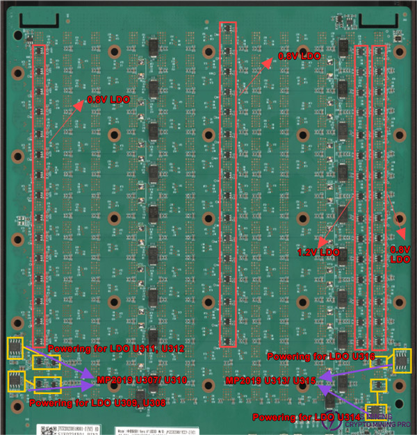
The VDDIO of the 1-16 domain chips is powered by 1.2V and 0.8V LDO chips. Each domain uses 4 LDO chips for powering: 1 LDO chip outputs 1.2V and 3 LDO chip output 0.8V. Each 0.8V LDO supplies power to 4 chips, as shown in the following figure.
For high-voltage domains 17 and 18, two MP2019s (U310, U307, U313, U315) output 2V in each domain to power LDO chip, which then supplies power to the chip VDDIO. LDO U311 and U312 (1.2 and 0.8V) are powered by U310 MP2019, LDO U308 and U309 (1.2 and 0.8V) are powered by U307 MP2019, and the other two MP2019s U313 and U315 output 2V to power two 0.8V LDO chips, a total of 2 groups, as shown in the following figure.
MP2019 location, LDO powering area diagram:
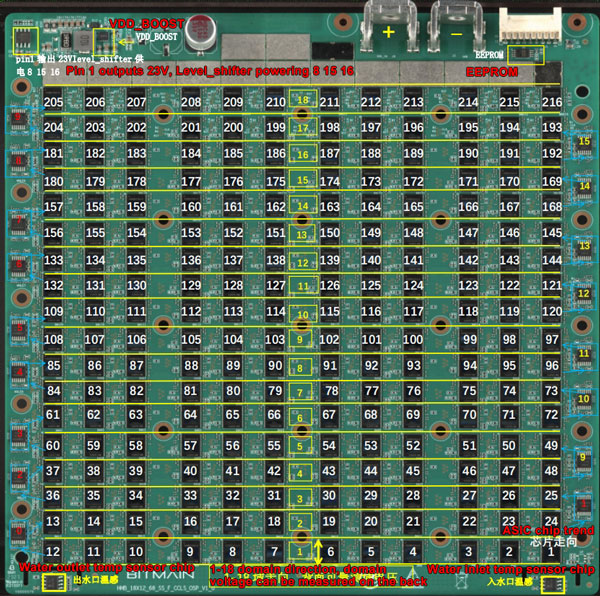
Compared with other models, the S21 hash board includes 17 level_shifters to perform addition operations on chip-related signals. A total of 17 level_shifters are used from the second domain to the last domain, as shown in the blue box in the following figure. Level_shifters 0-7 and 9-13 are powered by voltage across 5 domains. For example, level_shifter0 is powered by the voltage of the 5th domain, and so on. Level_shifter8, 14, and 15 are powered by MP2019 (U1). There are 2 temperature sensor chips (T0-T1), 1 each at the water outlet and water inlet, as shown in the following figure.
Hash board domain 18 direction (when testing PT3, the chip position in the kernel log starts counting from 0, asic 0-215, and the voltage domain also starts counting from 0, i.e. domain0-domain17).
Note: Compared with BM1362 and BM1398 on the hash board, the S21 hydro BM1368 hash board cancels the MOS and PIC circuits, adds 17 op amps, and performs signal addition operations starting from the second domain. Generally, if the PT1&PT3 test results are poor or the junction of the 2 domains is poor, the op amp can be checked first, including abnormal chip detection at 12M baud rate.
2. S21 Hyd. hash board boost circuit:
The boost is powered by the PSU VDD_IN and converted to 25V through U9, as shown in the figure.
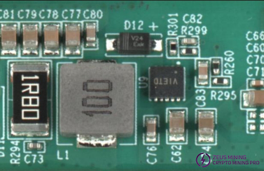
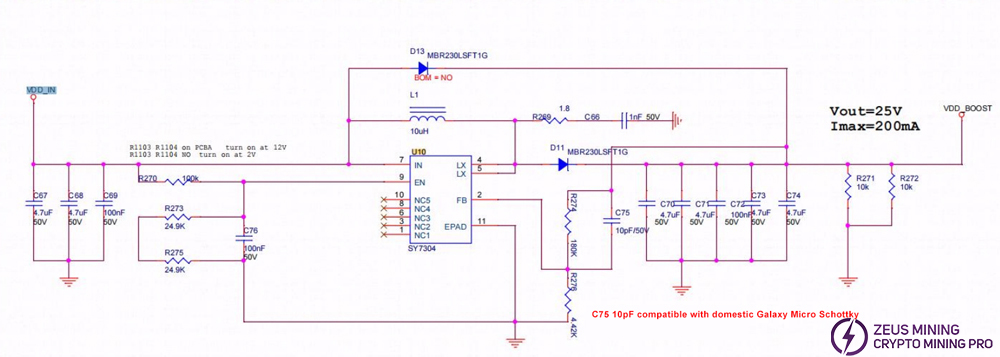
3. S21 Hyd. chip signal direction:
CLK signal flow: The signal generated by the Y1 25M crystal oscillator, travels from chip BM1 to BM216; the voltage is approximately 0.58V to 0.6V.
TX (CI, CO) signal flow: It enters from pin 7 of the IO port (3.3V), goes through level conversion IC U2, and then is transmitted from chip BM1 to BM216; it was measured by a multimeter to be around 1.1V.
RX (RI, RO) signal flow: From chip BM216 towards BM1, it returns to the signal ribbon terminal pin 8 via U1 and back to the control board; the multimeter measured it at around 1.1V.
BO (BI, BO) signal flow: From chip BM1 to BM216.
RST signal flow: It enters from pin 3 of the IO port, passes through R216, and then transmits from chip 01 to 216; it was measured by a multimeter to be around 1.2V.

4. Overall machine architecture:
The machine's overall architecture is mainly composed of 3 hash boards, 1 control board, and an APW111721X power supply.
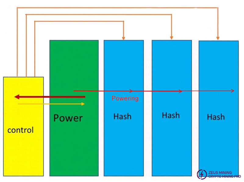
V. Hash board common fault phenomena and troubleshooting steps
1. Fault: The single board test detection chip is 0 (PT1 test)
Step 1: Check the power output.

Step 2: Check the domain voltage output. Measure the voltage domain to see if it is about 1.1V. If VDD_IN is powered, domain voltage is usually present. Measure the output of the power terminal of the hash board first.
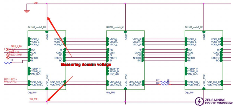
Step 3: check whether CLK is output. Measure the front and rear of BM1. If there has output, measure the last chip to see if there is CLK. If not, use dichotomy to repair it.
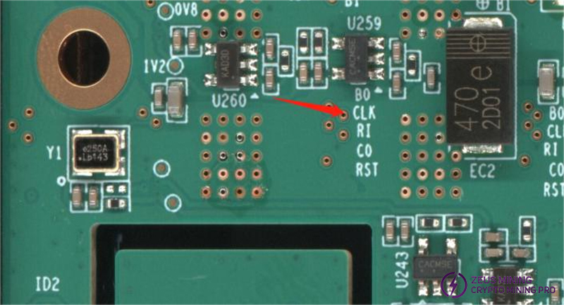
Step 4: Check each group of LDO 1.2V or PLL 0.8V output.
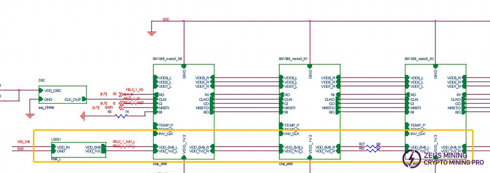
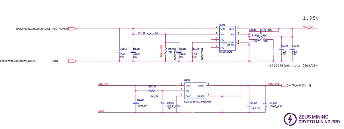
Step 5: Check the chip signal output (CLK/CI/RI/BO/RST).
Refer to the voltage range described in the signal direction. If the voltage value deviation is large during measurement, it can be compared with the measurement values of the adjacent group for judgment.
2. When the test fixture LCD displays EEPROM NG, check whether U6 is soldered properly;
3. When the test fixture LCD displays sensor NG, indicating abnormal temperature readings, follow these steps to troubleshoot:
A) Check the serial port log: if sensor=0, detect whether the U4, U5 chips or nearby SMD resistors and capacitors are soldered properly;
B) Sensor={0, 1}: corresponding sensor locations are {U4, U5}; Prioritize checking whether the 3.3V powering is normal, supplied from the control board to J1.
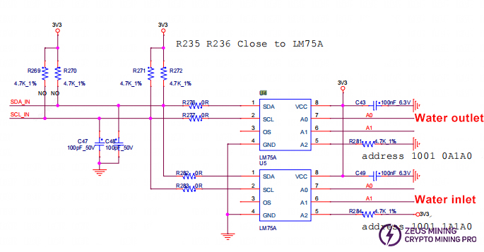
4. When the test fixture LCD displays INIT NG WATER_TEMP, indicating abnormal water temperature readings at the water inlet and outlet, check whether U4, U5 and the surface-mounted resistors and capacitors are soldered properly.
5. Fault: Incomplete chip detection on the single board - PT1 / PT3 (sweep) test:
a) If the LCD displays ASIC NG: (0), first measure the total domain voltage of 21V and the single domain voltage to ensure they are normal. Then, use a shorting probe to short the RO test point and the 1V2 test point between the first and second chips, and run the find chip program. Check the serial port log, if it still finds 0 chips, one of the following issues might be present:
a-1) Use a multimeter to check if the 1V2 and 0V8 test points have voltages of 1.2V and 0.8V respectively. If not, it could indicate an issue with the 1.2V or 0.8V LDO circuit in that domain, or the two ASIC chips in that domain are not well-soldered. Most issues are caused by a short circuit in the 1.2V or 0.8V surface-mounted filtering capacitors (measure resistance of related SMD filtering capacitors on both sides of the PCBA) or measure if the VDDIO to ground impedance is abnormal. If abnormal, disconnect the 1.2V and 0.8V resistors; two chips are a group. If the impedance or diode values remain abnormal after disconnecting the resistors, consider desoldering the corresponding chips.
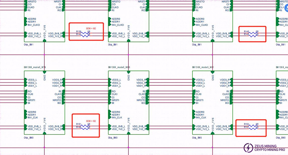
a-2) Check if there are any abnormalities in the U1 & U2 circuits, such as poor soldering of resistors.
a-3) After verifying that the 1V2 and 0V8 voltages are normal, sequentially check if the RO, RST, CLK, CI, and BI signals are functioning properly.
a-4) Abnormal water temperature or cooling issues can cause U4 and U5 to burn out, leading to no output from the 1.2V or 0.8V in the first domain, and BM1 and BM2 chips burning out (U4, U5 burnt out).
b) If one chip is found in step a), it indicates that the first chip and the preceding circuit are fine. Use a similar method to check the subsequent chips. For instance, if shorting the 1V2 test point and RO test point between the 38th and 39th chips shows 38 chips, then the first 38 chips are fine. If still no chips are found, first check whether the 1V2 is normal; if it is, then the issue lies with the chips after the 38th. Continue using a dichotomy until the problematic chip is identified. Suppose there is an issue with the Nth chip; shorting the 1V2 and RO between the N-1 and N chips finds the N-1 chip, but shorting between the N and N+1 chips does not find all chips.
c) If the LCD displays ASIC NG: (X, fixed report a certain chip), consider the following two scenarios:
c-1) First scenario: The test duration is roughly the same as that for good boards (typically, the X doesn't change each test). This situation is likely due to abnormal serial resistance soldering of the CLK, CI, and BO signals before and after the Xth chip, so focus on inspecting these six resistors. There is a small probability that abnormal soldering of the pins of the chips X-1, X, X+1 is causing the issue.
c-2) Second scenario: The chip's appearance is normal, and voltage signals are normal, which means the problem is with the chip itself.
6. Fault: Single board Pattern NG, meaning the reply nonce data is incomplete (PT3 station):
Pattern NG is caused by the characteristics of one or more chips being significantly different from others, currently caused by several types of defects:
1) If the chip die is found to be damaged, just replace the chip;
2) Chips with solder bridging, poor soldering (a domain with two chips reporting nonce returns of 0 or 1);
3) The voltage in this area is low, and the 1.2V and 0.8V voltages are normal, which means there is a problem with the chip itself;
4) Multiple chips or an entire domain returning abnormal nonce data; measure the domain voltage and troubleshoot starting from the domain with the low voltage.
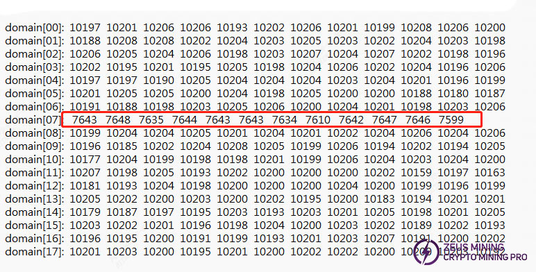
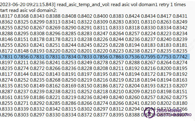
PS: It is important to note that the numbering for both domains and ASICs starts from 0.
As shown in the figure above, if an entire domain shows abnormal chip responses, initial analysis should be conducted from the test log. The BM1368 series chips support domain voltage and temperature printing features (Note that the domain voltage printed by domain adc is only about 0.82V because one of the small domains cannot be displayed, and approximately 0.28V should be added to obtain the correct value).
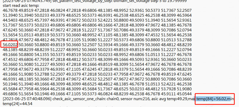
Furthermore, analyze the test log to see if there is any abnormal chip temperature. If one or several chips show abnormally high temperatures, prioritize checking if the heat sink is properly in contact with the chips, if there are foreign objects on the chip surface, or if the surface flux (after chip replacement, ensure to clean off any residual flux thoroughly) is not cleaned off, all of which can cause abnormal temperatures. To troubleshoot heat dissipation anomalies, first mass-produce chip temp_P/N. If any anomalies are found, the chip needs to be replaced.
7. Fault: Chip test OK, PT3 function test returns abnormally.
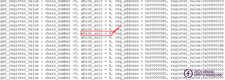
Repair method: During PT3 testing, observe the serial port print log. The issue is generally caused by a wrong register address in one of the chips, as shown in Figure 5-11, replacing the BM5 chip should resolve the issue (ASIC numbering starts from 0).
8. Phenomenon: PT3 first 6 domains nonces reply 0
Repair method: Check the appearance and measure the 6 domain chip signal impedance to see if it is abnormal. Generally, it is caused by chip short circuit or foreign matter;

9. Phenomenon: Phenomenon: When PT3 sweeps the frequency, the raising frequency detection chip reads 0
Repair method: Check the appearance. It is usually caused by a short circuit on the chip, or the resistor around the chip is connected with tin, or foreign matter;

10.Whole machine test R:1 defective
Log prompts find x asic (x represents less than 216), which means that the hash board chip is not found completely. If the PT1 chip is abnormal, it can be repaired. Chain0 represents board 1, Chain2 represents hash board 3, the hash board next to the power supply is chain2, i.e. hash board 3, and the middle one is Chain1, which represents board 2.

VI. Control board issues causing the following problems:
1. The entire machine does not operate:
1) Check if the voltages at several output points are normal; if there's a short circuit at 3.3V, first disconnect U8. If the short persists, remove the CPU and measure again. For other abnormal voltages, generally replace the corresponding voltage converter IC.
2) If voltages are normal, check the soldering condition of the DDR/CPU (checked via X-RAY at the production).
3) Try updating the flash program using an SD card;
To start the machine normally after a control board card flash, the following steps are needed:
a) After a successful card flash, the green LED indicator will stay lit; at this point, power off and restart;
b) Repower and wait for 30s (the process of activating OTP).
c) OTP (One Time Programmable) is a type of memory in the MCU, meaning it can be programmed only once: once the program is burned into the IC, it cannot be altered or erased again;
Precautions:
(1) If power is suddenly cut off during the OTP activation process or before 30 seconds have elapsed, it may cause the OTP activation on the control board to fail, and the control board will not start (will not connect to the network). In this case, U1 (the main control IC FBGA on the control board) needs to be replaced, and the replaced U1 should not be used on the Series 19 models again;
(2) U1 cannot be used on other series of models if the OTP function is enabled on the control board.

2. The entire machine cannot find IP
It is high probability that operational anomalies are causing the IP to not be found; refer to point 1 for troubleshooting.
Check the network port, network transformer T1, and the appearance and soldering of the CPU.
3. The entire machine cannot be upgraded
Check the network port, network transformer T1, and the appearance and soldering of the CPU.
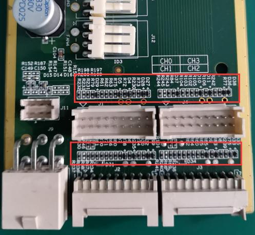
4. The entire machine fails to read the hash board or missing chain, showing error J:1
A. Check the connection status of the ribbon cables.
B. Check the control board parts corresponding to the chain.
C. Inspect the quality of the wave soldering of the header pins connectors and the resistance around the plug-in interfaces.
VII. Whole machine fault phenomenons
1. Initial testing of the whole machine
Refer to the test procedure document; issues generally arise from assembly process errors or control board manufacturing issues.
Common symptoms include failure to detect an IP and abnormal chain detection. If anomalies occur during testing, maintenance should be conducted based on prompts from the monitoring interface and the test LOG. The methods for initial testing and aging test repairs are consistent; repairs should be made according to the corresponding test item anomalies.
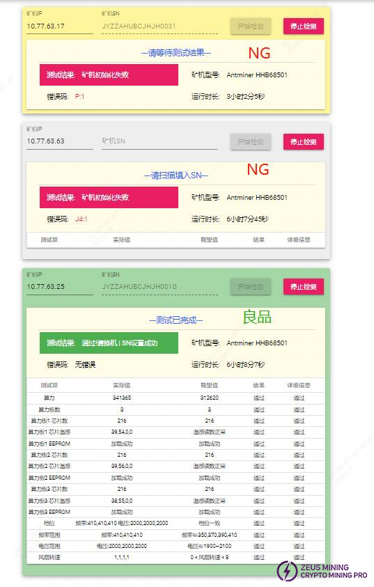
1) Phenomenon: P:1 (Prioritize checking if the water temperature is too high or if the water flow is normal; typically, temperatures exceeding the standard lead to overheating protection. If a specific chip is indicated for overheating protection, after checking the water temperature and flow, the hash board’s cooling should be inspected for abnormalities.)
2) Phenomenon: JX:1 (Bad ASIC chip; prioritize checking the cooling. If cooling is found to be normal, the chip itself is generally faulty.)
2. Aging test: During the aging test, maintenance should be conducted based on the monitored interface test, such as:
1) Missing chain: This typically means that one out of three boards is missing. In most cases, there is a problem with the connection between the hash board and the control board. Check the ribbon cables for any open circuits. If the connections are okay, test the single board with PT3 to see if it passes. If it does pass, the problem is likely with the control board. If it doesn't pass, use the PT3 repair methods to fix it.
2) Abnormal temperature: Usually, the issue is that the temperature is too high. Our monitoring system sets the maximum PCB temperature at 80 degrees Celsius and the chip temperature at 95℃. If temperatures exceed these limits, the machine will alarm and not operate normally. Typically, check if the water outlet temperature exceeds 45℃, which could cause high temperatures. Additionally, thermal grease can also cause abnormal temperatures.
3) Inability to detect all chips (OM firmware can boot and run, IM firmware cannot run; OM firmware hash rate is 2/3 or 1/3 of normal values): Check the log to see if it's due to an insufficient number of chips: if there aren't enough chips, refer to PT1&PT3 for testing and repair.
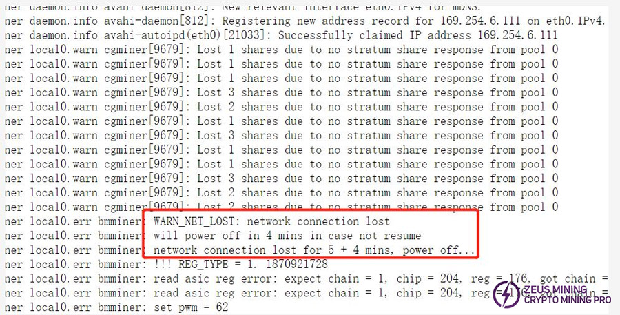
4) No hash rate after running for a period of time, pool connection interrupted: Check the network.
5) Aging test status of normal quality machine.
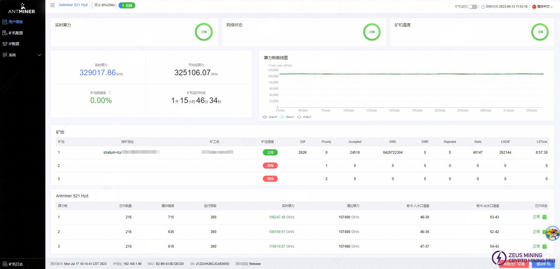
6) Whole machine hash rate drop R:1
After assembling the whole machine from single boards that tested OK, one of the boards shows a low hash rate: as shown in the following diagram, the first board loses its hash rate about 3 minutes into operation. Here’s how to analyze this issue:
First, perform a single board PT3 test to check if this board is OK. If the test fails to detect all chips, then repair the single board. If the board tests OK, take it out and run it separately with OM firmware, ensuring water inlet and outlet connections are made. When the board drops out again, measure the domain voltage or signals like CLK, RO, etc., which usually show abnormalities. Then, perform repairs targeting the locations where abnormalities were detected.
7) Whole machine running I2C error
Generally caused by issues with ribbon cable connections. Try restarting or re-plugging the ribbon cable.
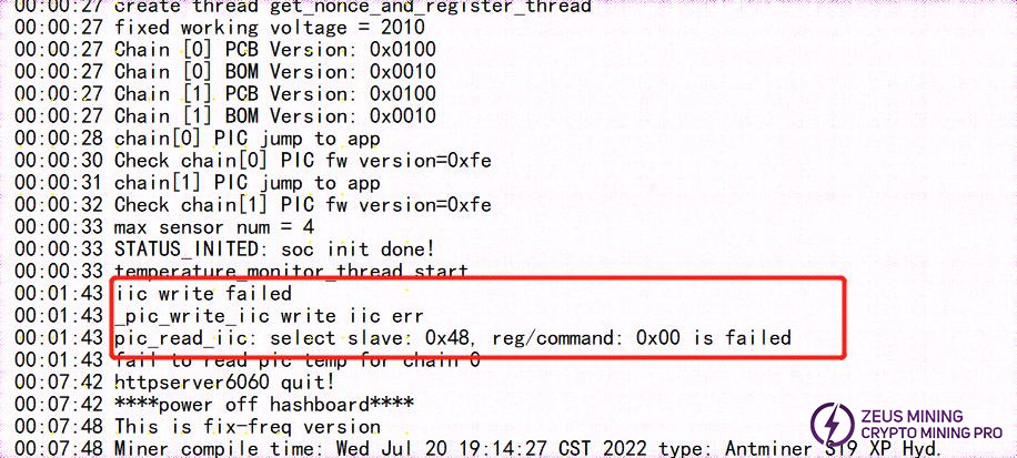
3. Construction of water cooling test platform for after-sales repair and production repair (test water temperature: 32℃ to 35℃, single board water flow rate 3 - 3.5L/min)
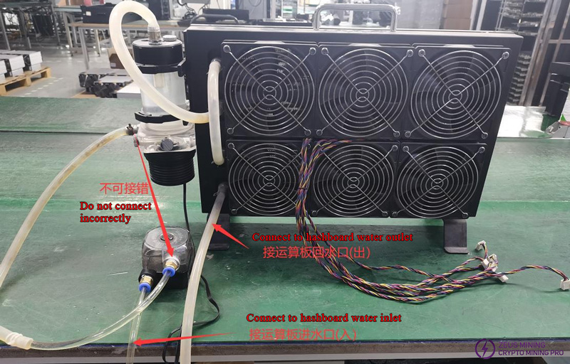

1) Due to the first generation water cooling radiator inadequate cooling capacity, an additional water pump needs to be added in series (or two water cooling radiator connected in series) during modification.
2) When modifying, use 8mm air pipe connectors and air pipes;.
3) If cooling is still insufficient, auxiliary air cooling fans can be added.
Refer to the troubleshooting steps at each station above. After repairs, use scan mode to test PT1, then proceed to test PT3.
VIII. Other considerations
Repair process diagram

Figure 8-1 Repair process chart
·Routine Inspection: First, visually inspect the hash board to check for PCB deformation or scorching; these issues must be addressed immediately. Check if any components show clear signs of burning, are displaced due to impact, or are missing; if found, address these issues first. If no problems are detected visually, proceed to test the impedance of each voltage domain to check for shorts or open circuits. Any issues discovered should be addressed before moving on. Next, check if all domains have a voltage of about 1.2V.
· After passing routine checks (routine short-circuit tests are essential to prevent damage to chips or other materials upon powering), use a test fixture to inspect the chips and make judgments based on the results.
· According to the display results of the test fixture detection, start from the vicinity of the faulty chip and detect the chip test points (CI/RST/RO/CLK/BI) and VDD0V8, VDD1V2 and other voltages.
· Follow the signal directions, except for the RO signal, which is transmitted in reverse (from chip 216 to 1), while signals like CLK, CI, BI, and RST are transmitted forward (from 1 to 216), to locate the faulty point by the order of power supply.
· When pinpointing a faulty chip, it needs to be re-soldered: Apply flux (preferably no-clean flux) around the chip, heat each solder joint of the chip pins to a molten state to allow the chip pins to re-mesh with the pads and collect solder, achieving a re-soldering effect. If the fault persists after re-soldering, consider replacing the chip.
· After the repair, the hash board must pass twice to be considered normal when tested with a test fixture. The first time, after replacing the parts, wait for the hash board to cool down, use the test fixture to test it, and then put it aside to cool down. The second time, wait a few minutes until the hash board is completely cooled, and then test it again.
· After the hash board is repaired OK, ensure to keep detailed repair/analysis records (repair reports should include: date, SN, PCB version, location, cause of defect, responsibility for the defect, etc.) for feedback to production, after-sales, and R&D.
· Once records are properly documented, reassemble into the whole machine for routine aging.
· Repaired goods that pass inspection must start from the first station in production (inspection should at least include appearance and begin at PT1/PT3 test stations).
· For repaired hash boards, the heat sink must be reprinted with thermal grease (otherwise it will cause temperature abnormalities).
We use cookles to Improve your online experience. By continuing browsing this website, we assume you agree our use of cookies.