


Antminer S21 Pro Hash Board Repair Guide
I. Requirements for Preparation of Maintenance Platforms/Tools/Equipment:
1. Platform Requirements:
An electrostatic mat maintenance workbench (the workbench needs to be grounded), along with anti-static wrist straps and proper grounding.
2. Equipment Requirements:
(1) A constant temperature soldering iron (with a temperature range of 350°C - 380°C). A pointed soldering iron tip is used for soldering small SMD components such as SMD resistors and capacitors.
(2) A hot air gun and a heating stage (with a temperature range of 350°C - 400°C), and a BGA rework station are used for the removal and soldering of chips/BGA.
(3) A multimeter, equipped with a soldering steel pin and covered with heat-shrinkable tubing for convenient measurement (Fluke 15b+ is recommended).
(4) An oscilloscope (FNIRSI-1013D oscilloscope is recommended).
(5) Network cables (Requirement: Connected to the Internet with stable network connection).
3. Requirements for Maintenance and Testing Tools:
(1) The S21 Pro PSU adopts APW171215a, with a voltage range of 12V - 15V, version V1.32, meeting safety regulations (calibrated), along with power adapter cables (self-made: use thick copper wire to connect the positive and negative poles of the PSU and the hash board. It is recommended to use 4AWG copper wires with a length within 60cm, which are only limited to use in PT1 and for maintenance and testing purposes). They are used for powering the hash board.
(2) The test fixture should use the testing jigs of V2.1 or V2.3 control boards (the part number of the test jig is ZJ0001000004). Discharge resistors need to be installed on the positive and negative poles of the test fixture's power port, using cement resistors of 20 ohms and above 100W. When using the 19 series universal test fixture for the first time, it is necessary to flash the B047 version of the jig firmware.
4. Requirements for Maintenance Auxiliary Materials/Tools:
(1) Solder paste (M705), flux, circuit board cleaner mixed with anhydrous alcohol. The circuit board cleaner is used to clean the residue of flux after repair.
(2) Thermal conductive gel: Fujipoly SPG-30B, which is used to be applied on the surface of the chip after maintenance.
(3) Ball planting steel mesh: BM1370 LGA with a chip size of 6mm x 8mm.
(4) Solder wick.
(5) Solder balls: The recommended diameter is 0.4mm. When replacing a new chip, it is necessary to apply solder to the pins of the chip before soldering it onto the hash board. After evenly applying the thermal conductive gel on the surface of the chip, then attach the large heat sink.
(6) Barcode scanner.
(7) Adapter board: TTL to RS232 serial port module.
(8) Self-made short-circuit probe (using pin wiring for welding).
5. Requirements for Common Maintenance Spare Parts:
(1) SMD resistor, 33 ohms, 1%, 1/20W, R0201 (0603).
(2) SMD resistor RES, 10K, ±1%, 1/16W, 0402.
(3) SMD resistor Res 0Ω, 1/16W, 0402, 5%.
(4) SMD ceramic capacitor Cap, 1uF, ±10%, 16V, X5R, 0402.
(5) SMD ceramic capacitor, 1uF, 6.3V, 20%, X5R, C0201 (0603).
(6) SMD ceramic capacitor Cap, 22uF, ±20%, 6.3V, X5R, 0603.
II. Maintenance Requirements:
1. When replacing chips, pay attention to the operation techniques. After replacing any components, there should be no obvious deformation on the PCB board. Check whether there are any problems such as missing components, open circuits, or short circuits on the replaced parts and their surrounding areas.
2. Maintenance personnel must possess certain electronic knowledge and have more than one year of repair experience. They should be proficient in the soldering techniques for BGA/QFN/LGA packaging.
3. After repair, the hash board must be tested more than twice and all tests must be OK before it can pass. Each work order has a corresponding number of hash board serial numbers (SN). Each board has a unique SN, during the maintenance and testing scanning process, the SNs cannot be scanned crosswise and cannot be reused.
4. Check whether the tools and tester can work normally. Determine the parameters of the testing software at the maintenance workstation, the version of the test fixtures, etc.
5. For the test of replaced chip, it is necessary to first test the chips. After passing the test, then conduct the PT3 frequency sweeping function test. During the function test, it must be ensured that the heat sink is assembled properly. When installing the heat sink, the thermal conductive gel must be evenly applied on the surface of the chip, and the fan needs to be connected to the fixture for controlled testing.
6. The single board does not have a fan for heat dissipation. If PT1 is tested continuously, the chip will overheat and burn the board;
7. When measuring signals and voltages with the heat sink attached, the measurement can be carried out while the fan on the TOP side is blowing air.
8. When replacing a new chip, use the maintenance stencil to print solder paste on the pins of the chip to ensure that the chip is pre-tinned before being soldered onto the PCBA for maintenance.
9. The test fixtures at the maintenance end are all used in the Test_Mode and tested in the scanning mode. After passing the test, the production end will start the flow line from the first testing station for normal machine assembly and aging (assembled according to the same level).
10. After the PCBA with the removed heat sink is repaired successfully, the heat sink must be re-glued before being installed for the subsequent flow line test (otherwise, it will cause poor operation of the whole miner).
III. Test fixture production and precautions (the tester should meet the heatdissipation of the hash board and facilitate signal measurement)
1. For the first time, use the A3HB70601 series test fixture SD card to update the FPGA of the fixture's control board. After decompression, copy it to the SD card and insert the card into the card slot; power on for about 1 minute and wait for the indicator to flash 3 times before the update is completed; (If it is not updated, it may cause a fixed report of a chip failure during the test).

2. Make the test SD card according to the requirements. For PT1 chip test and PT3 function test, directly decompress the compressed package to make the SD card. After decompression, delete the original Config file first. For example, the configuration file Config.PT1.ini is named Config.ini, and then click "Yes". The final configuration file is "Config.ini". (The repaired board must be re-tested from PT1 according to the production process. Repair personnel cannot skip the test line operation privately)
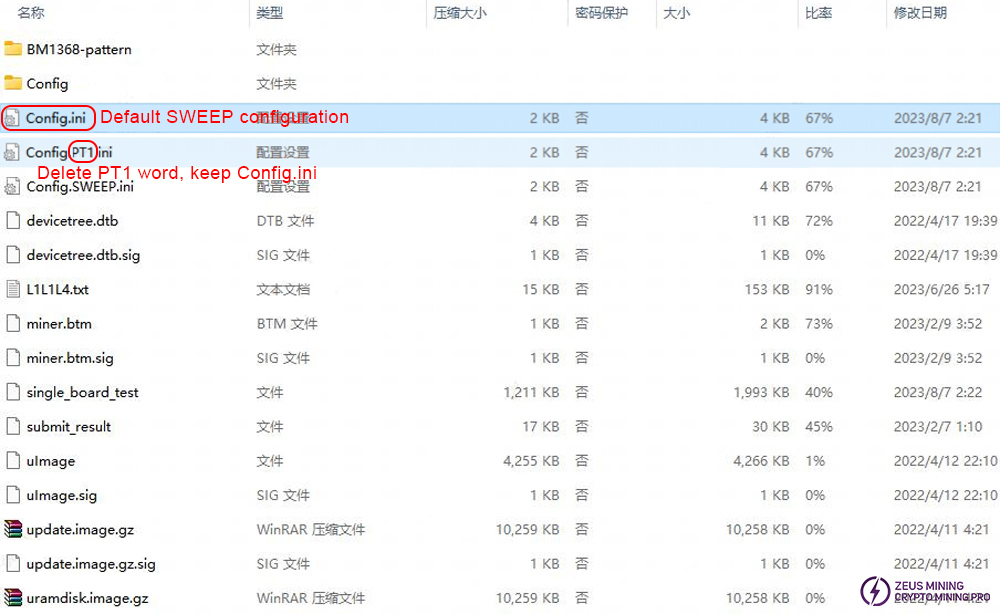
3. When testing the PT1 chip at the production, after-sales, and outsourced maintenance ends, a barcode scanner, serial port tool, and network cable are required. For details, see the A3HB70601 test process document.
IV. Principle Overview
1. S21 Pro A3HB70601 hash board structure:
The hash board consists of 65 BM1370 chips (PCB silk screen order BM1-BM65), divided into 13 groups (domains), each domain consists of 5 ASICs; the working domain voltage of the BM1370 chip used in the A3HB70601 hash board is about 1.04V.
The ASIC chip VDDIO of domains 1-11 is powered by 1.2V&0.714V LDO, and each domain uses 3 LDOs for powering (1 LDO outputs 1.2V, 2 LDOs output 0.7V);
And each domain of 12&13 high-voltage domains is powered by 2 MP2019 (U146, U160) outputs 2.5V to power LDO chip, and then the LDO supplies power to the chip VDDIO, where LDO U93 and U94 (1.2 and 0.7V) are powered by U160 (MP2019), and the other two LDOs U145&U147 are powered by 2.5V output from U146 (MP2019), for a total of 2 groups, as shown in Figure 4-2.
The hash board adds 12 level_shifters to perform addition operations on chip-related signals. A total of 12 level_shifters are used from the 2nd domain to the last domain, as shown in the blue box in the figure below. The schematic diagram is shown in Figure 4-3.
Level_shifter 0 is 6V, and 1-9 are powered by voltage across 5 domains. For example, level_shifter1 is powered by the voltage of the 6th domain, and so on, about 5V (level_shifter 2 VDD=7V (7-2GND=5V)) as shown in Figure 4-3.
Level_shifter10 and 11 are powered by U24 output VDD_LDO (as shown in Figure 4-5), and the input voltage of U24 is taken from the Boost circuit 19V0 as input, as shown in Figure 4-6.
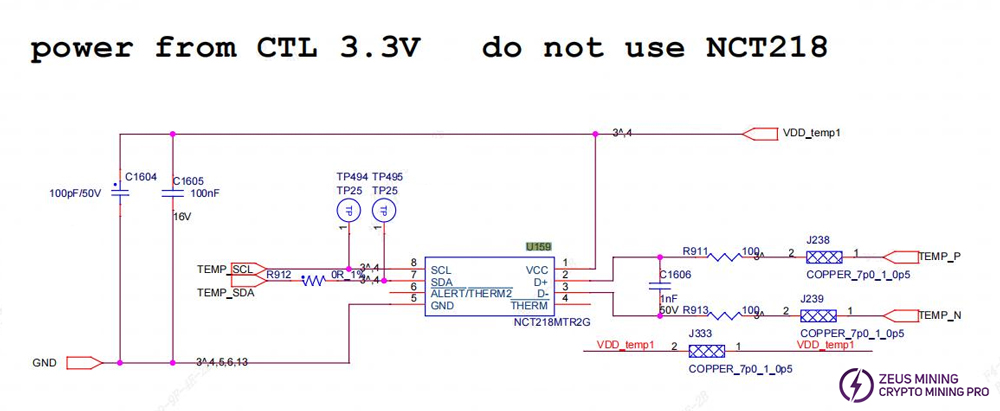
U19 is added to the temperature sensing circuit, which is a four-way bidirectional conversion switch controlled by the I2C bus. The SCL/SDA upstream pair is extended to four downstream channels to control the temperature sensing. U19 controls 3 isolated ICs (U18 and U20 and U22), U18 is powered by the 3.3V output form the control board, and U20&U22 takes the supply voltage across the domain, as shown in Figure 4-7. U154/U156/U158 temperature sensors are used to detect chip temperature, and the corresponding chip positions are shown in the figure below.
Each temp sensor is isolated and processed by its own isolation IC, and then output to the I2C four-way bidirectional conversion switch U19. Attention: The air inlet temperature sensor U159 is directly connected to U19.
The I2C four-way bidirectional conversion switch is responsible for managing the I2C communication between various devices. It can connect or isolate the I2C bus of different devices as needed to achieve data transmission and control.
The isolation IC processes the temperature signal from each sensor and passes the processed signal to the I2C four-way bidirectional conversion switch. The switch can select a specific channel according to the control signal and transmit the corresponding temperature data to the control board.
The control board can communicate with various devices through the I2C bus, including temperature sensors, isolation ICs, and conversion switches. Send control instructions to the conversion switch to select the temperature sensor data to be read and receive the processed data.
Hash board 13 domain direction: The chip position in the PT3 test log starts counting from 0, asic 0-64, and the voltage domain also starts counting from 0, that is, domain0-domain12.
Note: Compared with 1362 and 1398, 1370 cancels the MOS and PIC circuits, adds 12 operational amplifiers, and performs signal addition operations from the second domain. Generally, PT1 and PT3 is bad, or there is a bad situation at the junction of 2 domains, the operational amplifier can be checked first, including 12M baud rate chip detection abnormalities, etc.
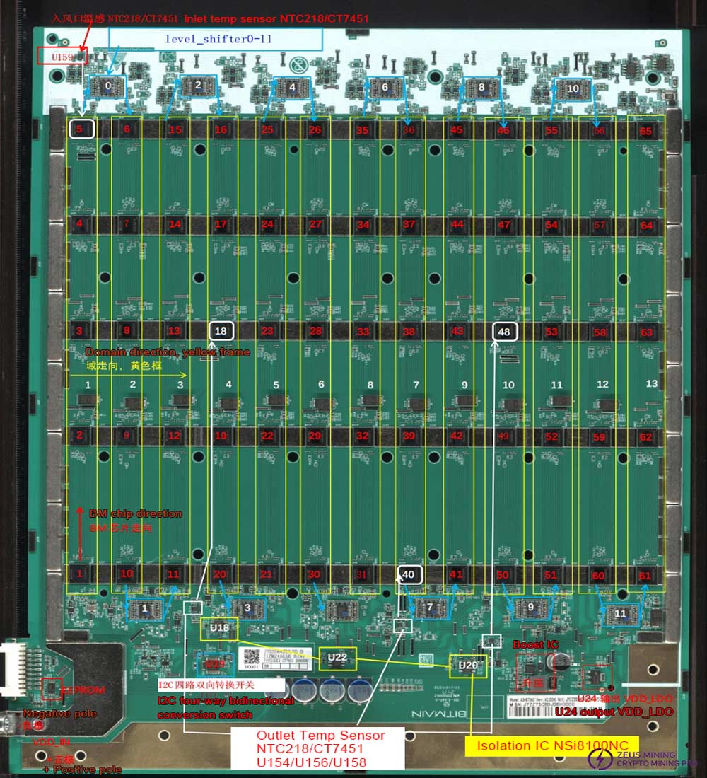
Figure 4-0
BM chip circuit diagram (one of them is captured):

Figure 4-1
MP2019, 1.2 and 0.7V LDO circuit schematics (two of them are captured):
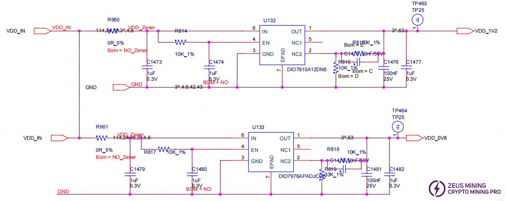
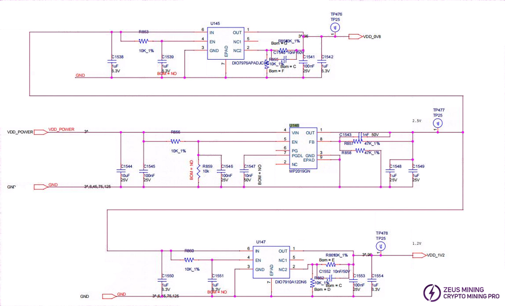
Figure 4-2
Level_shifter circuit schematic diagram (one of them is captured):
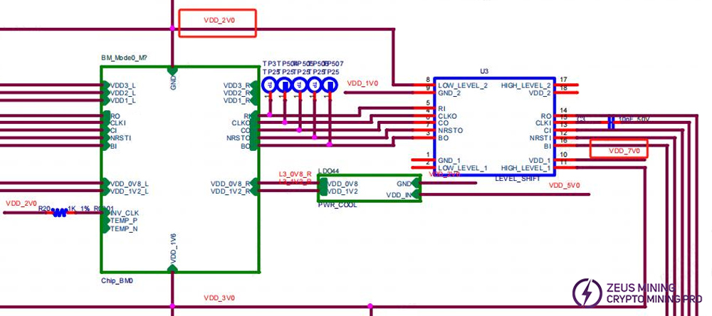
Figure 4-3
VDD_LDO powering schematic diagram:

Figure 4-5
BOOST circuit schematic diagram:

Figure 4-6
Schematic diagram of air inlet temperature sensor:
Four-way bidirectional conversion & chip temperature sensing circuit principle diagram:
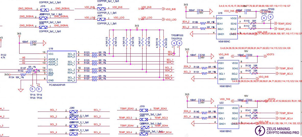
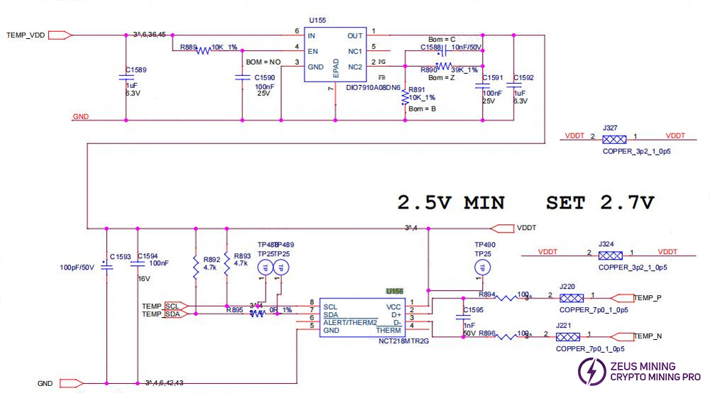
Figure 4-7
2. A3HB70601 hash board boost circuit:
The boost is powered by the powering VDD_IN and converted to 21V through U23, as shown in Figures 4-8 and 4-6.
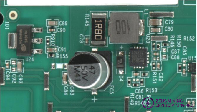
Figure 4-8
3. Signal flow of A3HB70601 chip:
(1) CLK signal flow is generated by Y1 25M crystal oscillator, Y1 is transmitted from chip BM1 to chip BM65, voltage is about 0.58-0.6V;

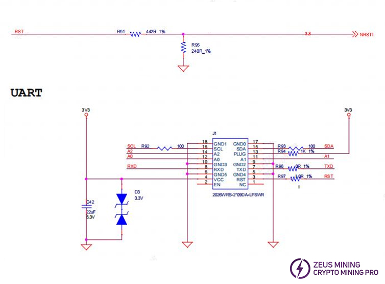
(2) TX (CI, CO) signal flow, from IO port 7 pin (3.3V) to level conversion IC U15, and then from BM1 chip to BM65 chip, the multimeter measured about 1.1V;
(3) RX (RI, RO) signal flow, from BM65 chip to BM1 chip, through U14 back to the signal cable terminal 8th pin and then back to the control board, the multimeter measured about 1.1V;
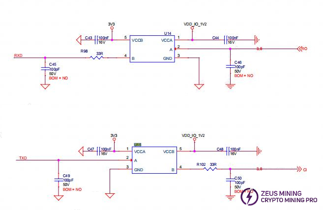
(4) BO (BI, BO) signal flow, from chip BM1 to chip BM65;
(5) RST signal flow, from IO port 3 pin, through R91 and then from chip 01 to chip 65, the multimeter measured about 1.2V;
4. Overall architecture
The S21 Pro is mainly composed of 3 hash boards, 1 control board, and APW17 power supply, as shown in Figure 4-4.

Figure 4-4
V. Common bad phenomena and troubleshooting steps of hash board
1. Phenomenon: Single board test detection chip is 0 (PT1 station)
Step 1: check the power output, please check Figure 4-6;
Step 2: check the voltage domain voltage output;
Measure the voltage domain voltage of about 1.04V to see if it is normal. If VDD_IN is powered, there is usually domain voltage. Prioritize measuring the power terminal output of the hash board.
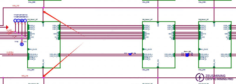
Step 3: check whether CLK is output. We can measure before and after BM1. If there is output, measure the last chip to see if there is CLK. If not, use the two-point method to repair it.

Step 4: Check each group of LDO 1.2V or PLL 0.7V output.

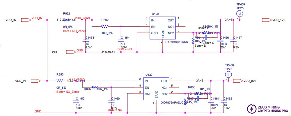
Step 5: check the voltage value range described by the chip signal output (CLK/CI/RI/BO/RST) reference signal trend. If the voltage value deviation is large during measurement, it can be compared with the adjacent group measurement value for judgment.
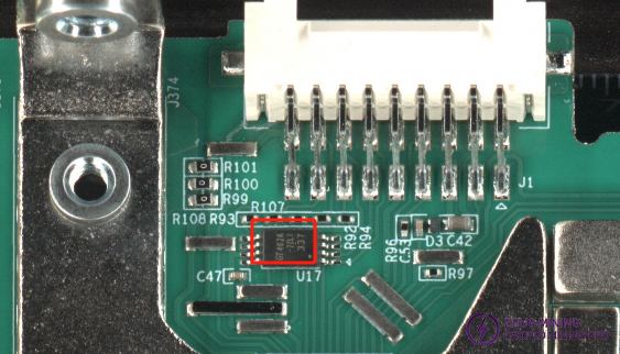
2. Phenomenon: EEPROM NG is displayed on the fixture LCD screen
Check whether U17 and surrounding components are soldered normally and whether the cable contact is OK;
3. Phenomenon: When the fixture LCD screen displays sensor NG, the test reading temperature is abnormal. Follow the steps below to troubleshoot:
A) Check the serial port log. If sensor=0, check whether the U159 chip or the adjacent SMD resistor and capacitor are soldered normally;
B) Sensor={0, 1, 2, 3}, the corresponding sensor position is {U159, U154, U156, U158}, we can check the corresponding position in Figure 4-0. If U18 is bad, pay attention to check whether the 3.3V powering is normal, which is output from the control board to J1.
4. Phenomenon: When the fixture LCD screen displays INIT NG TEMP, the test reads abnormal inlet and outlet temperatures.
Check whether the U159 powering and SMD resistors and capacitors are soldered normally.
5. Phenomenon: Incomplete chip detection on a single board (PT1/PT3 (sweep) station)
a) When the LCD displays ASIC NG: (0), first measure the total domain voltage to about 15V and the single domain voltage to be normal, then use a short-circuit probe to short the RO test point and the 1V2 test point between the 1st and 2nd chips, and then run the chip search program. Look at the serial port log. If 0 chips are still found at this time, it will be one of the following situations:
a-1) Use a multimeter to measure the voltage of the 1V2 and 0V8 test points to see if they are 1.2V and 0.7V. If not, it may be that the 1.2V and 0.7V LDO circuits of this domain are abnormal, or the two ASIC chips of this domain are not soldered properly. Most of the time, it is caused by a short circuit of the 0.7V and 1.2V SMD filter capacitors (measure the resistance of the SMD filter capacitors related to the front and back of the PCBA) or measure whether the ASIC chip VDDIO to ground impedance is abnormal. If it is abnormal, disconnect one of the chips. If the impedance or diode value is still abnormal after disconnecting the resistor, remove the corresponding ASIC chip.
a-2) Check whether the U1 & U2 circuit is abnormal, such as resistor cold soldering, etc.
a-3) After 1V2 and 0V8 are normal, measure RO, RST, CLK, CI, BI signals in turn to see if they are normal;
a-4) The fixture 3.3V short circuit is abnormal, the fan is abnormal or the heat dissipation is abnormal, which will cause U5 and U7 to burn out. If similar defects occur, first measure whether the 3.3V impedance to ground is abnormal. If it is short-circuited, remove the short-circuited component first, and install the corresponding components after the impedance returns to normal.
b) If 1 chip can be found in step a), it means that the 1st chip and the previous circuit are OK, and the binary method can be used for repair positioning. If the 1V2 test point and the RO test point between the 38th and 39th chips are short-circuited, and the log can find 38 chips, then the first 38 chips are fine (if 0 chips are still found, first check whether the 1V2 is normal, generally the chips after the 38th have problems). You can continue to use the binary method to check until the problematic chip is found. (Assuming that the Nth chip has a problem, then when the 1V2 and RO between the N-1th and Nth chips are short-circuited, the N-1 chip can be found, but when the 1V2 and RO between the Nth and N+1 chips are short-circuited, it reports 0, which means that the Nth chip is abnormal).
c) When the LCD displays ASIC NG: X (fixed reporting of a certain chip), there are two situations:
c-1) The first situation: the test time is basically the same as the OK board, and the X value usually does not change each time the test is performed (the test time refers to the time from pressing the start test button to the LCD displaying the result ASIC NG: X).
This situation is most likely caused by abnormal soldering of the CLK, CI, and BO series resistors before and after the Xth chip, so just focus on checking these 6 resistors. A small probability is that it is caused by abnormal soldering of the pins in the three chips X-1, X, and
X+1;
c-2) The second situation: There is no abnormality in the appearance of the chip, and the voltage signal is normal. It is a problem with the chip itself;
6. Phenomenon: Single board Pattern NG, i.e. the reply nonce data is incomplete (PT3 station).
Pattern NG is caused by the fact that the characteristics of some chips are quite different from other chips. Currently, there are several causes of defects:
1) If the chip die is found to be damaged, you only need to replace the chip;
2) The chip is tinned or the chip is poorly soldered (the reply number of nonce of two chips in one domain is 0 or 1);
3) The domain voltage of this domain is low, 1.2V & 0.7V voltage is normal, and the chip itself has problems;
4) Multiple chips or the whole domain nonces reply abnormally, measure the domain voltage, and check from the domain with low domain voltage.
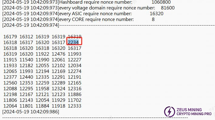
Figure 5-5
PS: Special attention should be paid to the fact that domain and asic numbers both start from 0.
As shown in Figure 5-5, if the whole domain chip responds abnormally, we need to conduct a preliminary analysis from the test log. The BM1370 series chips do not support domain voltage and temperature printing functions.
Secondly, check whether the chip temperature in the log is abnormal. If the temperature of one or several chips is abnormally high, first check whether the contact between the radiator and the chip is normal, whether there are foreign objects on the chip surface, and whether the surface flux after repairing and replacing the chip (the residual flux on the surface must be cleaned when repairing and replacing the chip) is not cleaned up, resulting in abnormal contact with the import glue, which will cause temperature abnormality. Check that there is no problem with heat dissipation first, and mass produce chip temp_P/N. If there is an abnormality, the chip needs to be replaced.
7. Phenomenon: The first 6 domains of PT3 nonces reply 0.
Repair method: Check the appearance and measure whether the signal impedance of the 6 domain chips is abnormal. Generally, it is caused by chip short circuit or foreign matter.

8. Phenomenon: When PT3 sweeps the frequency, the chip reads 0 after the frequency is increased.
Repair method: Check the appearance. During the trial production, it is generally found that the chip is short-circuited, or the resistors around the chip are tinned, or foreign matter is caused.

9. Phenomenon: R:1 is bad in the whole machine test, and the log prompts find x asic (x represents less than 65): It means that the hash board chip is not found completely. Use PT1 to check the chip abnormality and repair it. Chain0 represents board No. 1, Chain2 represents board No. 3, the hash board next to the PSU is chain2 No. 3, and the middle one is Chain1 represents board No. 2.
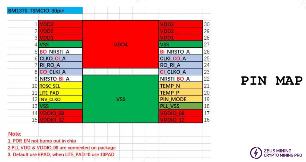
10. When the PT1 chip batch is abnormal, please refer to the PIN pin diagram below and use the ohm range of the multimeter to measure the corresponding impedance output.
VI. Control board problems lead to the following problems
1. The whole machine does not run
1) Check whether the voltage of several voltage output points is normal. If 3.3V is short-circuited, U8 can be disconnected first. If it is still short-circuited, the CPU can be unplugged and measured. For other voltage abnormalities, the corresponding voltage conversion IC is generally replaced.
2) If the voltage is normal, please check the welding condition of DDR/CPU (X-RAY inspection at the production end)
3) Try to update the flash program with SD card:
If the miner with control board card flashing needs to start normally, the following operations are required:
a) After the card flash is successful, the green LED indicator is always on, turn-off the power and restart;
b) Wait for 30s after powering on again (the time process of opening OTP);
c) OTP (One Time PRXgramable) is a type of memory of MCU, which means one-time programmable: after the program is burned into the IC, it cannot be changed or cleared again.
Note:
(1) If the power is suddenly cut off or the time is less than 30 seconds during the OTP process of the 7007 control board, the OTP function of the control board will fail, and the control board will not start (not connected to the Internet). U1 (control board main control IC FBGA) needs to be replaced. The replaced U1 can no longer be used in the 19 series.
(2) For control boards that have the OTP function turned on, U1 cannot be used on models of other series.
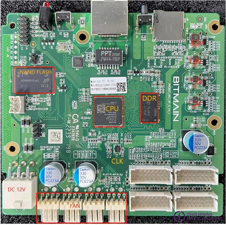
7Z007 Control Board
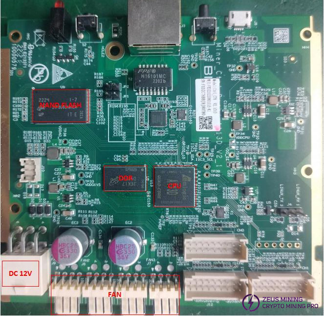
Amlogic Control Board
2. The whole machine cannot find the IP
(1) It is likely that the IP cannot be found due to abnormal operation. Refer to point 1 for troubleshooting.
(2) Check the appearance and soldering condition of the network port, network transformer T1, and CPU.
3. The whole machine cannot be upgraded
(1) Check the appearance and soldering condition of the network port, network transformer T1, and CPU.
4. The whole machine fails to read the hash board or the chain is missing
A. Check the connection condition of the cable.
B. Check the parts of the corresponding chain of the control board.
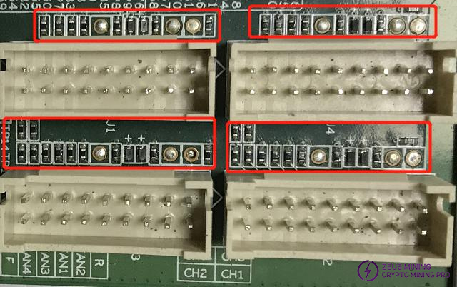
C. Check the wave soldering quality of the power strip pins and the resistance around the plug-in interface.
VII. Whole machine failure phenomenon
1. Whole machine initial test
Refer to the test process document, the general problems are assembly process problems and control board process problems.
Common phenomena: IP cannot be detected, abnormal number of detected fans, abnormal chain detection. If an abnormality occurs during the test, repair should be carried out according to the monitoring interface and test LOG prompts. The maintenance methods of the whole machine initial test and aging test are the same.
2. Aging test:
1) Fan display abnormality: Check whether the fan is working normally, whether the connection of the control board is normal, and whether the fan circuit of the control board is abnormal.
2) Less chain: Only 2 of the 3 hash boards can be identified. In this case, there is a problem with the connection between the hash board and the control board. Check the cable to see if there is an open circuit. If the connection is OK, the single board can be tested with PT1/PT3 to see if it can pass. If it can pass the test, it can basically be determined that it is a problem with the control board. If the test is NG, repair it according to the maintenance method of PT1/PT3.
3) Temperature abnormality: First check whether it is caused by high ambient temperature. The maximum PCB temperature in the monitoring system cannot exceed 81 degrees, and the chip temperature cannot exceed 98 degrees. If it exceeds 81 degrees or the chip temperature exceeds 98 degrees, the miner will report R:1 and cannot operate normally. Secondly, check whether the fan speed is abnormal. Low speed can also cause temperature abnormality. If it can be determined that the temperature of 1pcs hash board is abnormal, check whether the temperature sensor of the hash board is abnormal (S21 Pro has only two temperature sensors), and refer to the single board repair.
4) The whole miner detection chip is incomplete: disassemble the single board and retest PT1, and repair it according to the PT1 repair method.
5) There is no hashrate after running for a period of time, and the mining pool connection is interrupted. Check the network.
6) Aging test status of normal good quality machine:
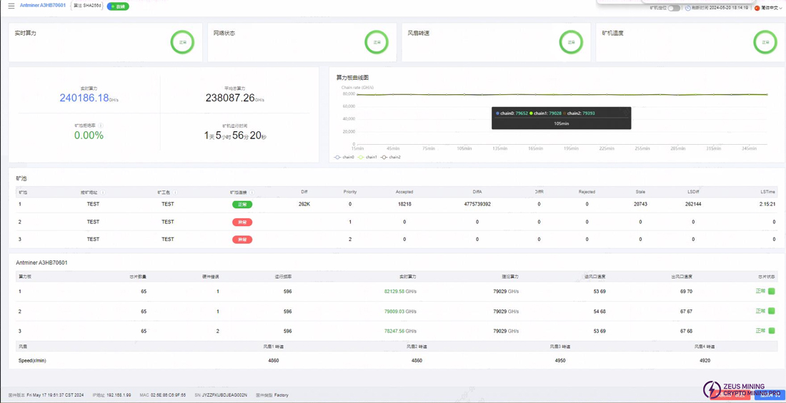
7) The hash rate of the whole machine drops JX:1;
a. First check the web page of the miner and the whole machine log to see if there are any chips with an X and a red report. If it is confirmed that there are 1 or more chips, we can first read the chip temperature through port 6060 after the web page IP, and determine whether the domain voltage is abnormal. If the temperature of the chip with an X is abnormal, first check the heat dissipation. The domain voltage abnormality can correspond to whether the impedance of the mass-produced chip is abnormal.
b. If the chip temperature and domain voltage are normal, one of the multiple chips is reported as bad asic. For the part that cannot be repaired, verify and retest PT3 OK, and the statistical data is fed back to the quality engineering for processing.
8) If an I2C error occurs during the operation of the whole machine, it is usually a cable contact problem. You can restart or re-plug the cable.
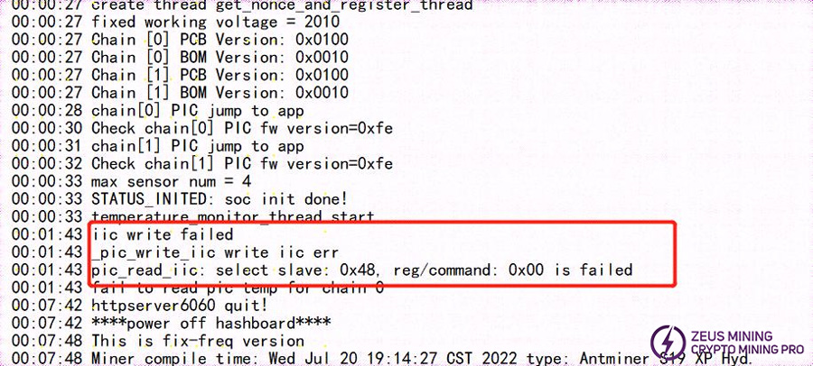
3. After-sales maintenance, production maintenance PT1 test platform construction (the test requires the fan to blow air up and down to dissipate heat).
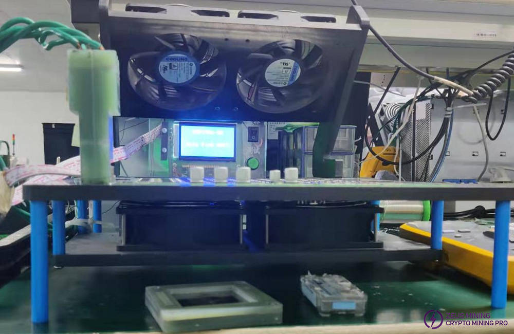
Refer to the above troubleshooting steps for each station. Please communicate with the after-sales engineer for details on the relevant test procedures and test fixtures. After maintenance, use the code scanning mode to test PT1 and then test PT3.
Ⅷ. Other precautions
Maintenance flow chart

1. Routine Inspection: First, visually inspect the hash board to check for PCB deformation or scorching; these issues must be addressed immediately. Check if any components show clear signs of burning, are displaced due to impact, or are missing; if found, address these issues first. If no problems are detected visually, proceed to test the impedance of each voltage domain to check for shorts or open circuits. Any issues discovered should be addressed before moving on. Next, check if all domains have a voltage of about 1.2V.
2. After passing routine checks (routine short-circuit tests are essential to prevent damage to chips or other materials upon powering), use a test fixture to inspect the chips and make judgments based on the results.
3. According to the display results of the test fixture detection, start from the vicinity of the faulty chip and detect the chip test points (CI/RST/RO/CLK/BI) and VDD0V8, VDD1V2 and other voltages.
4. Follow the signal directions, except for the RO signal, which is transmitted in reverse (from chip 65 to 1), while signals like CLK, CI, BI, and RST are transmitted forward (from 1 to 65), to locate the faulty point by the order of power supply.
5. When pinpointing a faulty chip, it needs to be re-soldered: Apply flux (preferably no-clean flux) around the chip, heat each solder joint of the chip pins to a molten state to allow the chip pins to re-mesh with the pads and collect solder, achieving a re-soldering effect. If the fault persists after re-soldering, consider replacing the chip.
6. After the repair, the hash board must pass twice to be considered normal when tested with a test fixture. The first time, after replacing the parts, wait for the hash board to cool down, use the test fixture to test it, and then put it aside to cool down. The second time, wait a few minutes until the hash board is completely cooled, and then test it again.
7. After the hash board is repaired OK, ensure to keep detailed repair/analysis records (repair reports should include: date, SN, PCB version, location, cause of defect, responsibility for the defect, etc.) for feedback to production, after-sales, and R&D.
8. Once records are properly documented, reassemble into the whole machine for routine aging.
9. Repaired goods that pass inspection must start from the first station in production (inspection should at least include appearance and begin at PT1/PT3 test stations).
10. For repaired hash boards, the heat sink must be reprinted with thermal grease (otherwise it will cause temperature abnormalities).