Contents of this book: It mainly describes the troubleshooting of various faults of the Z15 hash board, and the accurate positioning using the test fixture.
Scope: Applicable to all Z15 production, after-sales, and outsourced maintenance sites.
I. Requirements for maintenance platform:1. Constant temperature electric soldering iron (370℃-400℃) and pointed soldering iron tip are used for soldering small patches such as chip resistors and capacitors.
2. Portable desoldering gun and BGA repair station are used for chip disassembly and welding. Be careful not to heat for a long time to avoid PCB foaming.
3. APW3/APW3+/APW5 power supply (output 12V, 140A Max) and power adapter cable (made by yourself) are used for the test and measurement of the hash board.
4. Fluke multimeter, tweezers, V9 test fixture tool (conditional configurable oscilloscope).
5. Add anhydrous alcohol to flux and board washing water; board washing water is used to clean the flux residue and appearance after maintenance.
6. Tin tool, Tin tool steel sheet, solder paste; When replacing a new chip, the surface pads of the PIN pins of the chip need to be washed flat, and the chip should be soldered with a BGA repair station after tinning.
7. Antminer thermosetting adhesive applied to the chip/heat sink after repair.
II. Job requirements:1. Maintenance personnel must have specific electronic knowledge, more than one year of maintenance experience, and be proficient in BGA/QFN/LGA packaging and welding technology.
2. After maintenance, the hash board must be tested more than two times, and all are OK before passing!
3. Pay attention to the operation method when replacing the chip. After replacing any accessories, the PCB board has no obvious deformation. Check the replaced parts and the surrounding parts for open and short circuits problems.
4. Determine the maintenance object and the corresponding test software parameters and test tools.
5. Check whether the tools and test fixture can work usually.
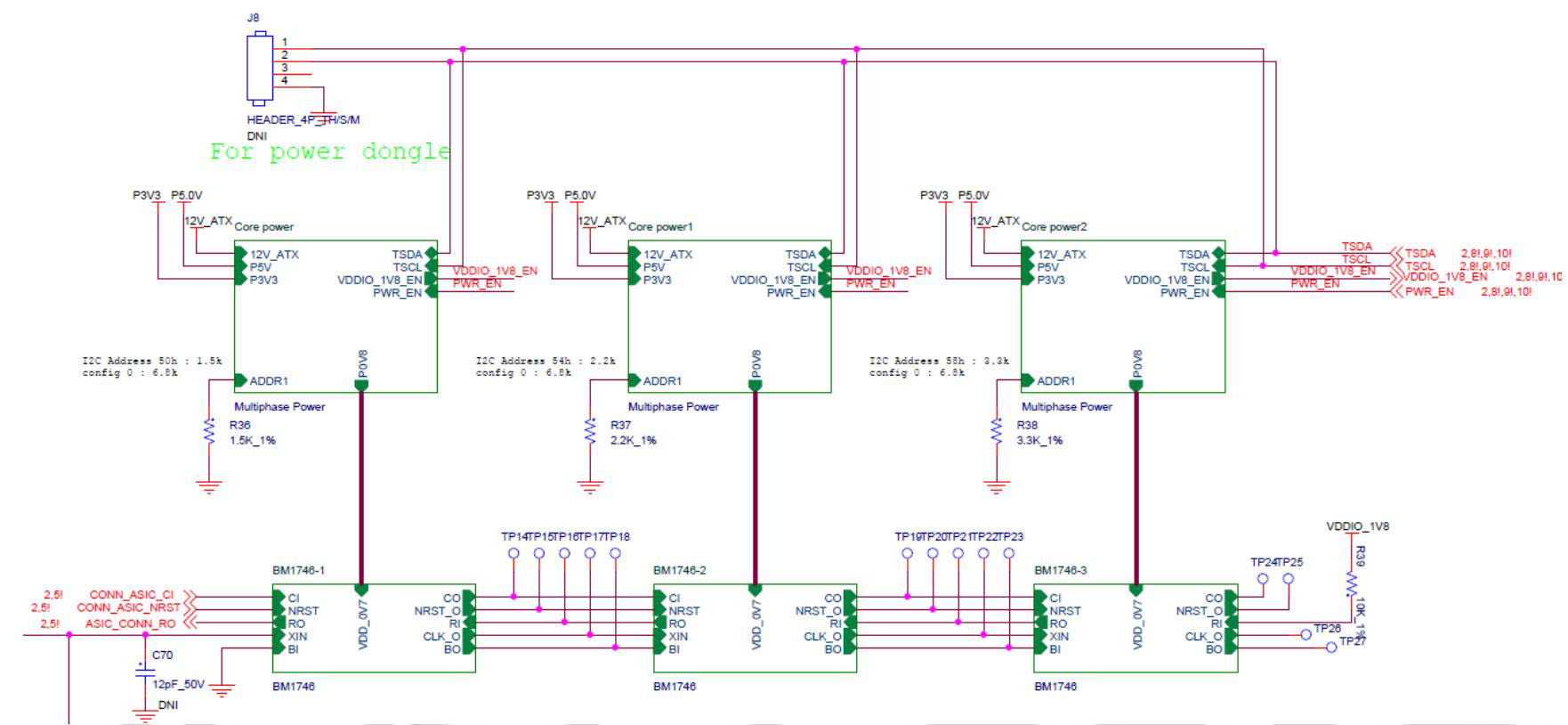
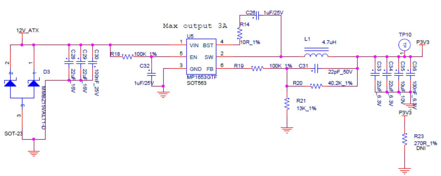
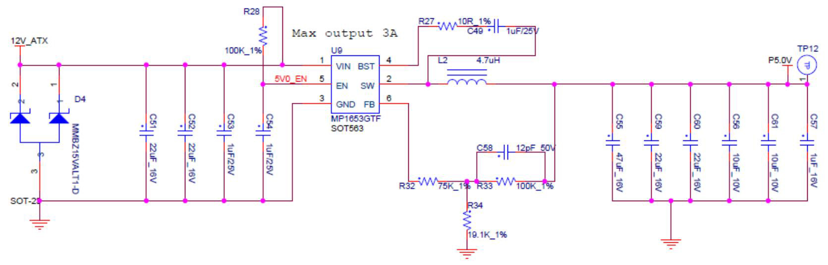
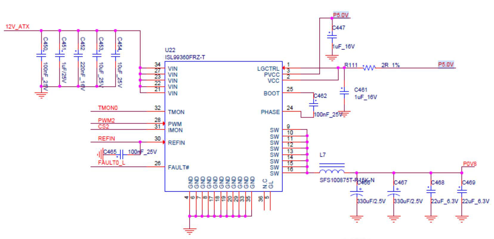
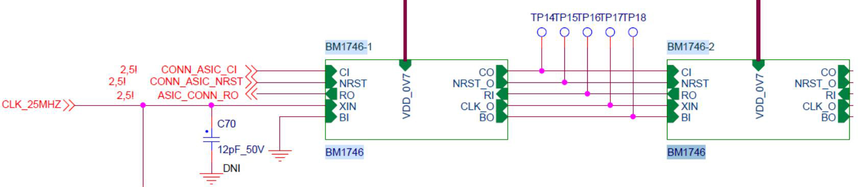
III. Principle and structure:1) Z15 consists of three BM1746 chips, each of which is controlled by a separate power management IC.
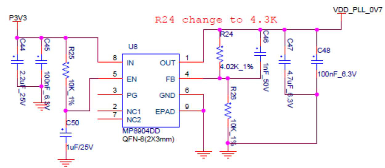
2) The working voltage of the BM1746 chip used by Z15 is 0.78V, and the chip has LDO to provide VDDIO 1.8V and VDDPLL 0.7V power supply.
3) The Z15 clock is a 25M crystal oscillator transmitted from the first chip to the third chip in series.After the repair and replacement of the chip has passed the test, it is necessary to apply the thermal paste evenly on the IC surface and tighten the screws to ensure that the heat sink is in contact with the chip to achieve heat dissipation.There are test points on the chip surface of the PCB board. For maintenance during production, if there is no heat sink, please use a fan to dissipate heat to the PCBA during the power-on test and analysis process. It is recommended to use low frequency 200M for inspection and maintenance, and the low-frequency test passes the post-installed heat sink and tests according to the default frequency value.
2. Signal direction of Z15 hash board:CLK (XIN) signal flow, generated by Y1 25M crystal oscillator, transmitted from chip 01 to chip 03; during operation, the voltage is 0.85V.
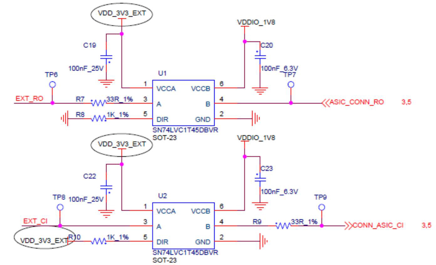
The TX (CI, CO) signal flows, from the IO port 7 pin (3.3V) into the level conversion IC U2, and then from the 01 chip to the 03 chip transmission; when the IO line is not inserted, the voltage is 0V, and the power supply during operation voltage 1.8V.
RX (RI, RO) signal flow direction, from chip No. 03 to chip No. 01, through U1 to the signal cable terminal, pin 3 and back to the control board; the voltage is 0.3V when the IO signal is not inserted, and the voltage during operation is 1.8V.
BO (BI, BO) signal flow, from chip No. 01 to No. 03; the multimeter measures 0V.
The RST signal flows in from IO port 3 and then is transmitted from chip 01 to chip 03; no IO signal is inserted; it is 0V in standby and 1.8V in operation.
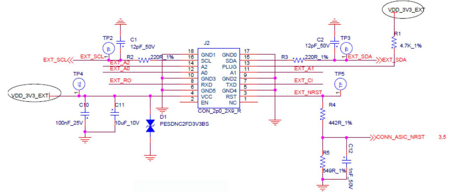
 3. The critical circuit of the Z15 hash board
During maintenance, mainly test 10 signal voltages before and after the chip (five before and after the chip: CLK, CO, RI, BO, RST); CORE voltage; LD0-1. 8V, PLL-0.7V; 12V to 5V voltage.
Detection method (each chip has a lead-out test point):
Plugin the I0 line, press the test fixture test button, and the PIC work. At this time, the normal voltage of each test point should be:
CLK: 0.85V
CO: 1.6-1.8V.
RI: 1.6-1.8V, when the voltage is abnormal or too low, the hash board will be abnormal, or the hash rate will be 0.
BO: 0V when no hash operation is performed, and 0V when hash operation is performed.
RST: 1.8V. The reset signal will be output again every time the test fixture's test key is pressed.
When the above test point status and voltage are abnormal, please infer the fault point according to the circuit before and after the test point.
IV. The failure and performance of the lousy phenomenon:1. The LDO 1.8V or PLL 0.7V is abnormal. The single-board shows that the chip is not fully read, and the data is crossed; the whole miner shows that the chip is missing, the board is dropped, or the chip is crossed.
2. The working voltage of the chip (the corresponding value can be measured according to the config setting value, the default value is 0.78V) is abnormal, this is a fault phenomenon: the number of chips read by the single board performance is abnormal; the whole miner lacks chips or loses the board.
Please check PIC soldering and programming. Please check the corresponding power management IC soldering and programming. Check whether the MOS of the corresponding group (the circuit is the same, only one circuit example is listed) is short-circuited.
1)If there is a replacement power management IC, please follow the steps below for online programming
a. Power controller firmware (there is no program download address, the maintenance party needs to apply for program requirements with the docking department)
The download line programming program (general maintenance general) is as follows
BEZ36601_PWR_V0.2.hex
b. Download tool
Intersil PMbus download cable and interface sequence are as follows:
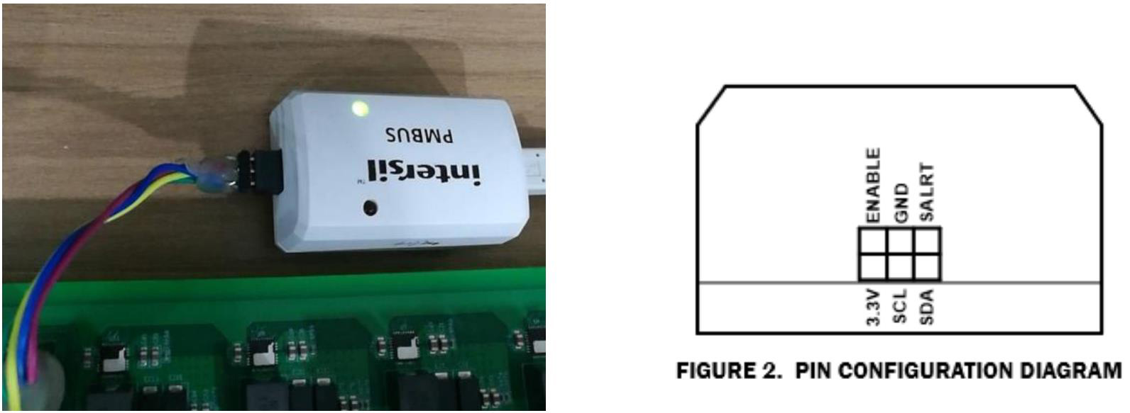
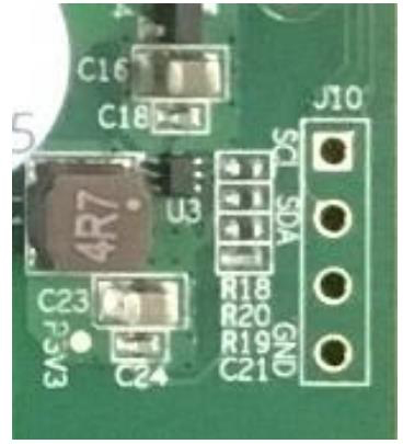
The cable of download cable is connected to J10 of the PCB (position 2 in the figure below), and it needs to be connected to GND, SDA, and SCL.
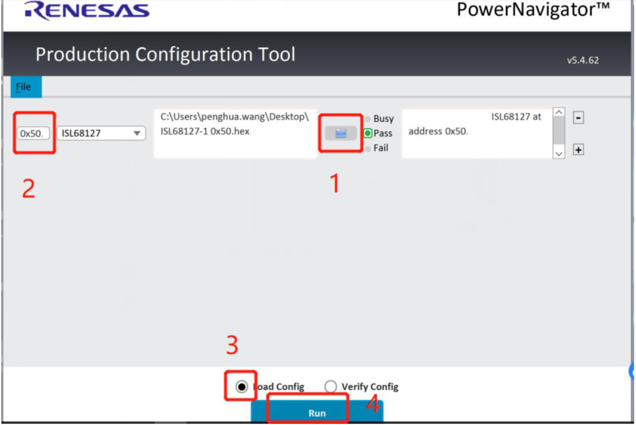
c. Burning software
Run the Production Configuration Tool, click position 1 to select the latest firmware BEZ24601_V03.hex, and then change position 2 to 0x50 (set according to the corresponding chip address:
The address of No. 01 chip is set to 0x50, the address of No. 02 chip is set to 0x54, and the address of No. 03 chip is set to 0x58), select the load config in position 3, and finally, click Run to enter programming.
Note: The power management IC only has a lifespan of 8 programming times; please program with caution.
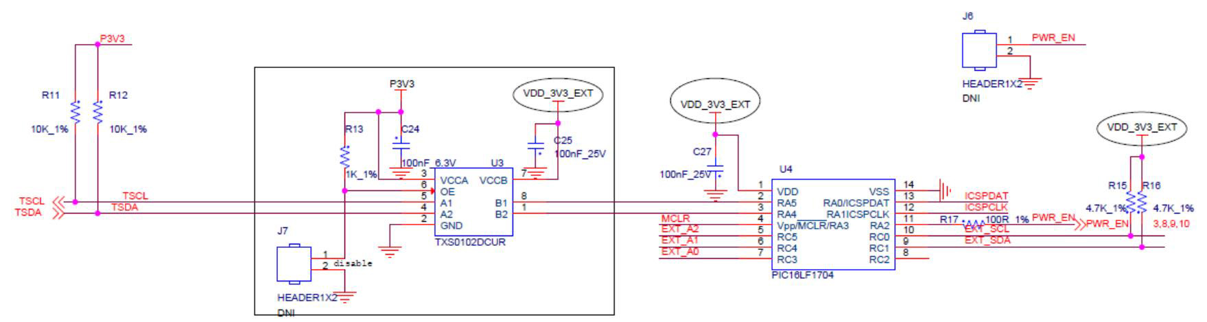
2)Burn the PIC program of the hash board.
a. Procedure
PIC16LF1704-BM1840-APP.X.production-1903081005-V4.hex
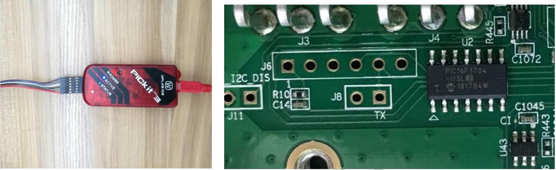
b. Download tool
PICkit3, pin 1 of the PICkit3 data cable corresponds to pin 1 of J3 on the PCB board, only need to connect pins 1, 2, 3, 4, and 5.
c. Burning software
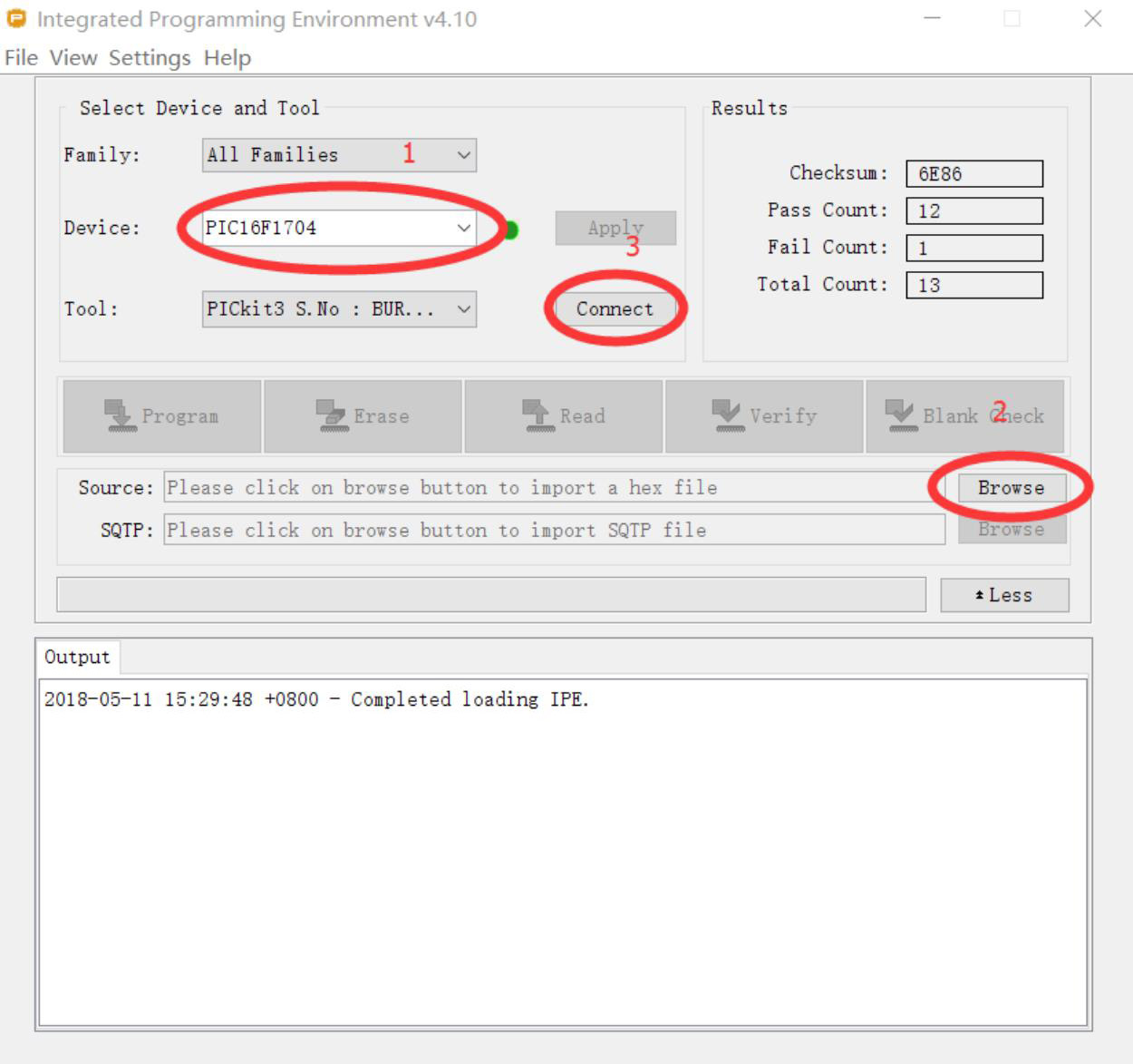
Open MPLAB IPE, select ①device: PIC16F1704, click ②Browse to select the .hex programming file, then click ③connect, the connection is standard, then click program and press button, click verify after completion, and it will prompt that the verification is completed to prove that the burning is successful.
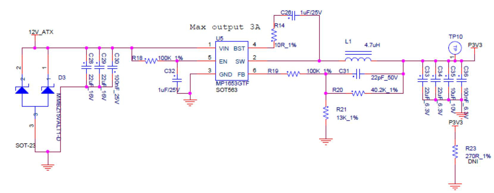
3. 3.3V abnormal or no output. Please check 3.3V related circuits. Check to solder first and make sure there are no shorts to the ground.
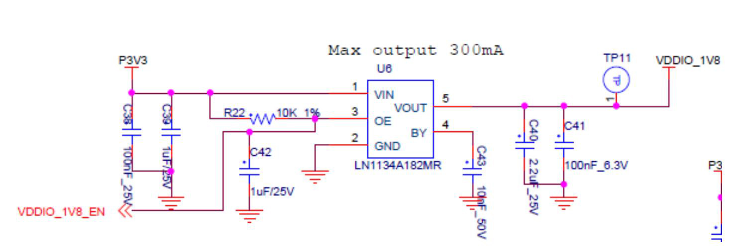
4. 5V is abnormal, refer to the above "1" point, 12V output is normal, such as 5V has no short circuit to ground (no short circuit corresponding to MOS tube), correspondingly check U6 welding, If there is no abnormality in welding, the material can be replaced; if there is a short circuit, some circuits and parts of the parallel MOS need to be checked.
5. The chip signal pin output is abnormal (BO/RST/CO/RI/CLK). Determine the wrong position according to the signal direction.
First, please power off to measure the chip-to-ground impedance (compared with the excellent board or adjacent group). Then, if possible, you can use X-RAY to check the welding effect of the chip.
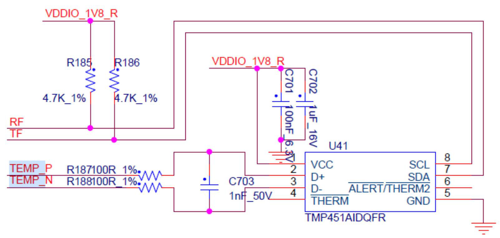
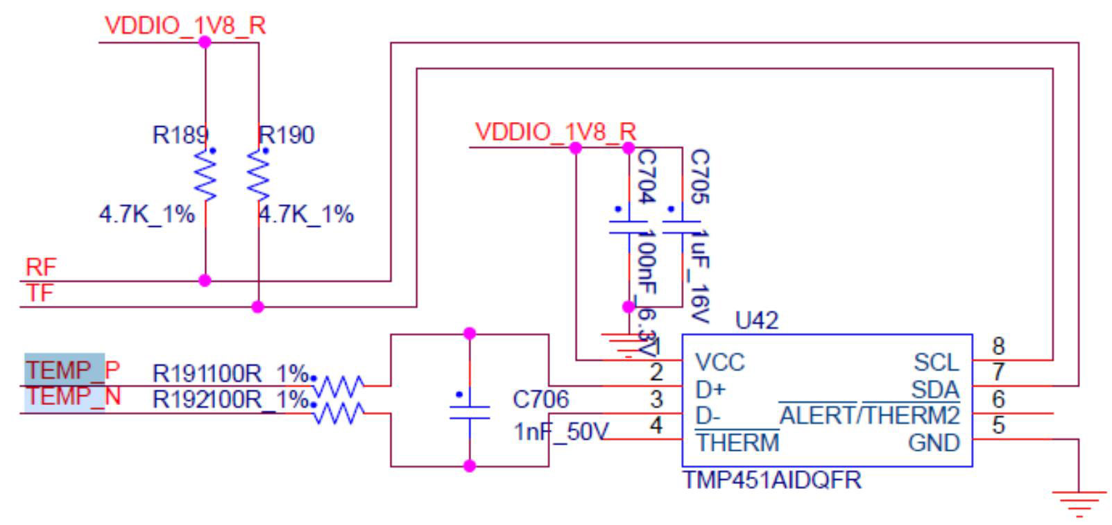
6. The temperature reading is abnormal. The bad board is shown as temp NG (the fixture interface can display temp NG and the log synchronization test result); the whole machine shows that the temperature reading is 0°C or no temperature can be read.
The temperature is sensed to the corresponding BM1744 chip. Therefore, please check whether the temperature sensor chip welding, temperature sensor working voltage, etc. are normal for the fault.
7. The returned nonce is insufficient, which is a fault phenomenon. The performance of the single board is that the number of nonces returned by a particular chip is insufficient; the whole machine shows that the error rate is high or the chip is crossed. Please check the soldering according to the bad chips displayed in the log; after checking that there is no problem with the soldering around the chip, it is recommended to re-solder the chip or replace the corresponding NG chip.
Note: The chip with an abnormal return value can be seen in the test fixture interface and the abnormal display "X."
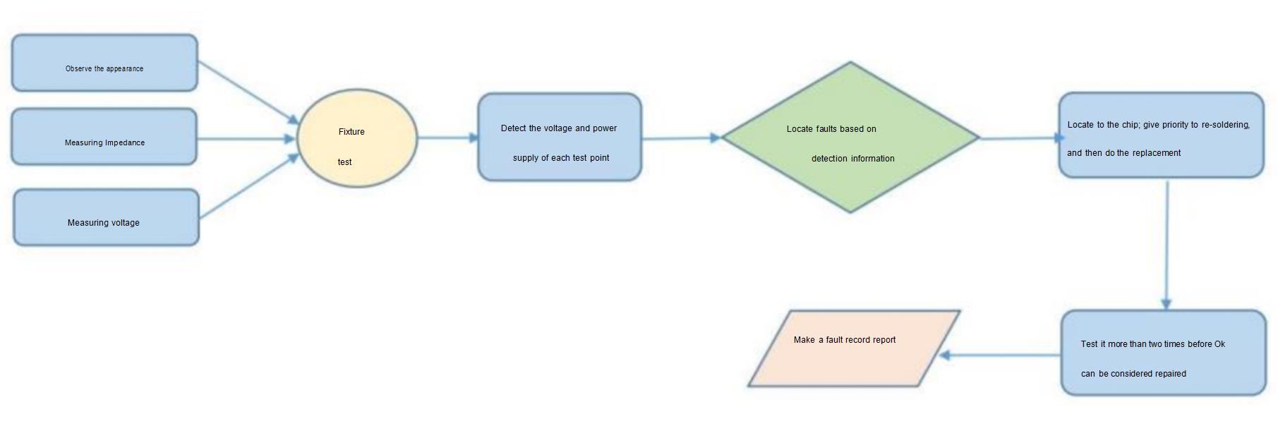
1. Routine detection: First, visually inspect the hash board to be repaired to observe any PCB deformation or scorching. If there is, it must be dealt with first; next, check whether there are parts with noticeable burn marks, parts impact offset, missing parts, etc. Secondly, after the visual inspection is no problem, you can first test the impedance of each voltage domain to detect whether there is a short circuit or an open circuit. If found, it must be dealt with first. Last, check whether the voltage of each group has 0.78v, and if a group does not measure 0.78V, you need to troubleshoot programming problems or MOS abnormalities.
2. After the routine inspection is OK (generally, the short-circuit inspection of the routine inspection is necessary to avoid burning the chip or other materials due to a short circuit when the power is turned on), the chip can be inspected with a test fixture, and judge the fault location according to the test result of the test fixture.
3. According to the display results of the test fixture, start from the vicinity of the faulty chip and detect the chip test points (CO/NRST/RO/XIN/BI) and voltages such as VDD0V8 and VDD1V8.
4. According to the signal flow, except the RX signal is transmitted in the reverse direction (chips 3 to 1), among which several signals CLK CO BO RST are transmitted in the forward direction (1-3), and the abnormal fault point is found through the power supply sequence.
5. When locating the faulty chip, the chip needs to be re-soldered. The method is to add flux (preferably no-clean flux) around the chip and heat the solder joints of the chip pins to a dissolved state to promote Re-run the chip pins and pads and close the tin. To achieve the effect of re-tinning. The chip can be replaced directly if the fault is still the same after re-soldering.
6. After repairing the hash board, when testing the test fixture, it must pass more than two times before being judged as a good product. For the first time, after replacing the parts, please wait for the hash board to cool down, use the test fixture to test the pass, and put it aside before cooling. The second time, wait a few minutes for the hash board to cool down completely before testing. The time interval between the two tests is only a few minutes, not affecting work efficiency.
7. After the hash board is repaired and OK. Relevant maintenance/ analysis records are required.