


Chip soldering skills
1. Tin on Chip
Apply a thin layer of flux to the chip with a brush;
2. Put tin on the chip pins (add solder flux to dilute the solder paste and stir evenly), use tweezers to apply a little solder paste evenly on the chip; Add a little solder paste to the two large pads in the middle on both sides of the pins. Be careful not to fill the solder paste.
3. Melting tin on the heating table on the chip, the working temperature of the heating table is controlled within 270℃, the chip is easy to be damaged if it exceeds this temperature.

4. Disassemble the chip
Apply flux to the chip pins with a brush, place the relevant parts of the hashrate on the heating platform until the tin is melted, and use tweezers to remove the core, the film is removed. The parts of the hash board that do not need to be welded should not be heated on the platform to reduce the temperature damage to the board and components.
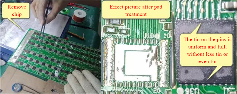
5. Pad processing
After the old chip is removed, use tweezers to apply a little tin on the pad. Be careful not to apply too much. After the tin melts, it adheres to the pad. Use the tip of the tweezers to move the pad back and forth to make the tin on the pad even and flat.
6. Install the chip
Clamp the soldered chip with tweezers to the accurately aligned pad, and heat it on the heating table to melt the tin, the chip and the pad, the tin is melted and combined and automatically straightened to complete the soldering. The soldered pins are required to be evenly filled with no less tin and no continuous tin. Wear gloves during welding operation to prevent high temperature burns.
Test platform installation and use
1. The hardware structure is shown in the figure:
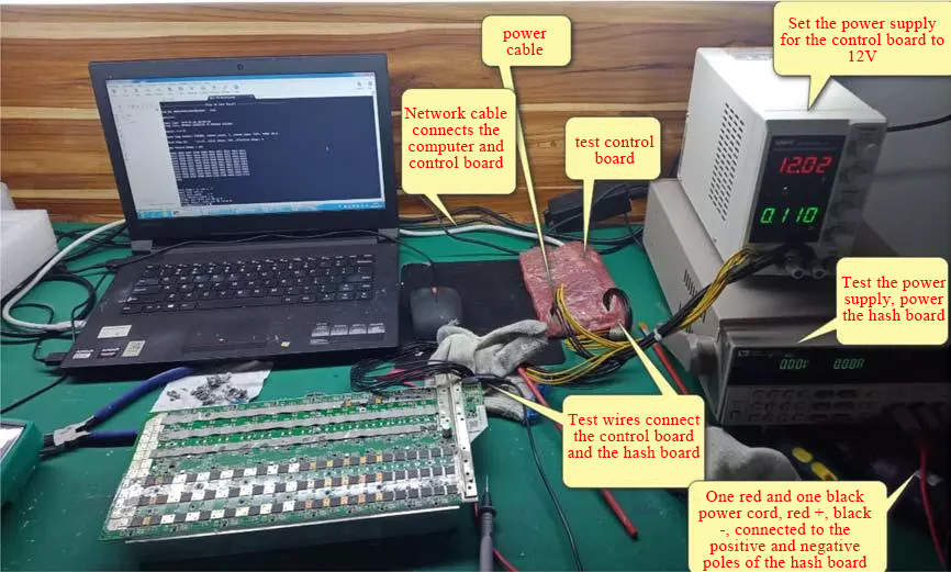
Software build
1. Double click

2. Click

3. Click
4.
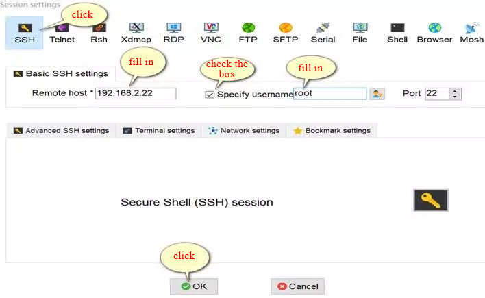
5. Fixed computer IP address
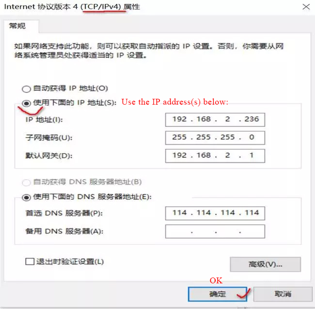
6. The following interface appears, you can start the hash board test
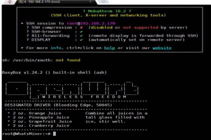
7. The test command is mainly test-readchipid (chip read) , Reboot (restart the control panel) ,echo 0> /sys/class/gpio/gpio99/value (or echo 0> /sys/class/gpio/gpio197/value, RST signal set low level 0V) echo 1> /sys/class/gpio/gpio99/value (or echo 1> /sys/class/gpio/gpio197/value, RST signal set high level 1.8V).
M20S power board circuit principle
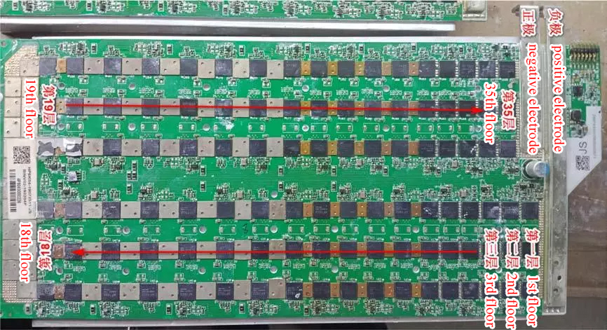
The main power supply relationship of the chip:
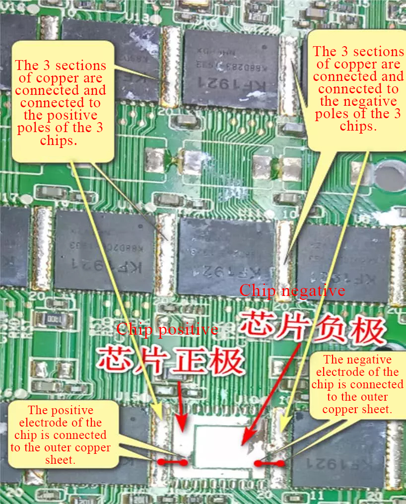
Every three M20S hash boards form a voltage domain. The positive poles of the three chips are connected together, and the negative poles are also connected together.
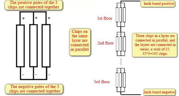
The power supply of three chips in each layer forms a parallel relationship.
Simplify the power supply model of each layer, and the interlayer voltage is the chip power supply voltage. The power supply relationship between layers is Tandem.
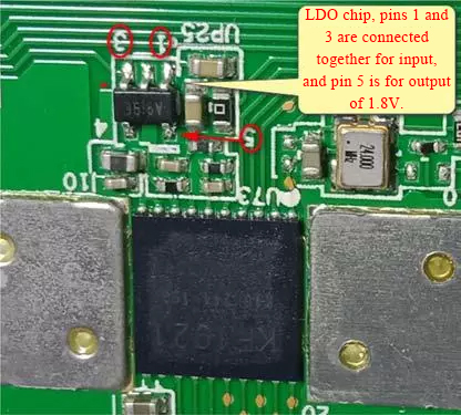
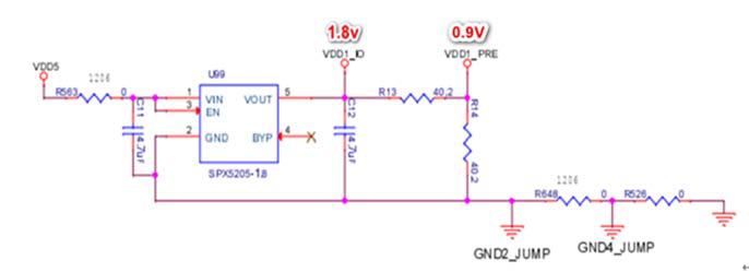
The LDO power supply relationship of the chip. The LDO supplies power for the normal signal transmission of the chip. Each layer has an LDO chip.
For power supply, pin 5 is the output, voltage 1.8V, then divided by 0.9V, and sent to the chip. When measuring, the benchmarks found by the fluke 15b+ multimeter are all the grounds of the current layer.
Signal flow chart
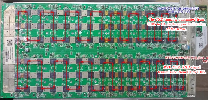
There are 5 transmission signals in the hash board, RST (reset), CLK (clock), CTSI (chip select), RXD (receive), TXD (send) Shooting), where RST, CLK, RXD, TXD are the main measurement signals.


The way the signal passes through the chip: straight in and straight out.
For example, measure a certain signal to judge whether the chip is bad, the input signal of the chip is normal, but the output is abnormal.
The chip is damaged. Measuring chip signals can directly measure the corresponding test points on the top and bottom of the chip or directly measure the corresponding leads on the top and bottom of the chip foot.
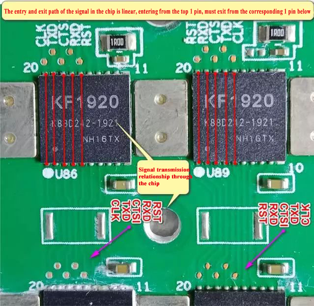
Conditions for the normal working of the hash rate chip

Memory and temperature sensor chip
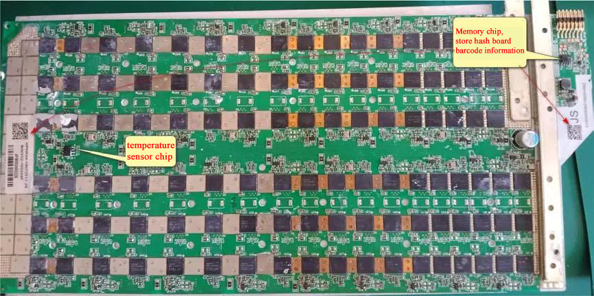
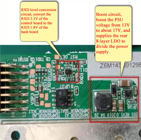
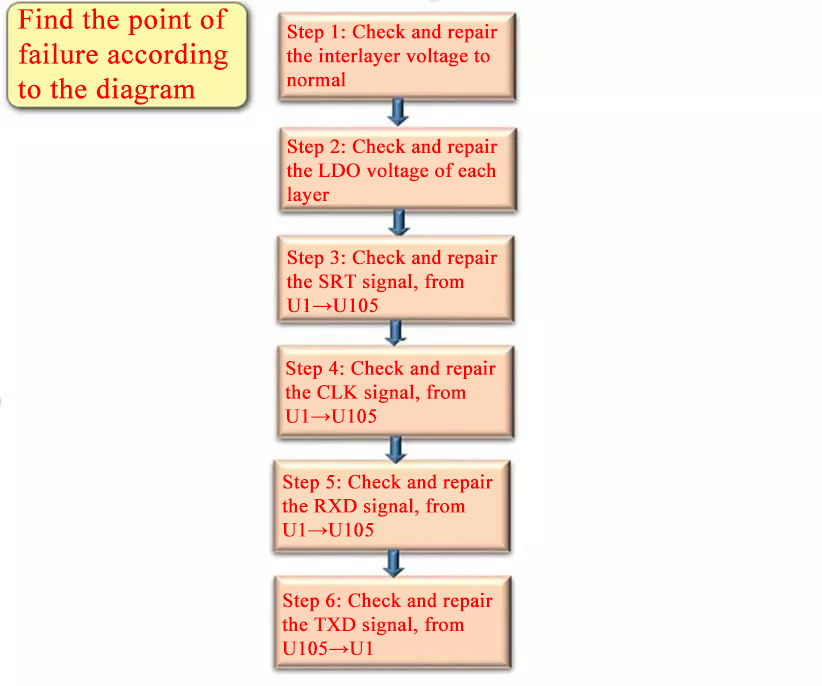
Maintenance ideas
Maintenance experience:
1. The reset fails and the LED light is on
During the test, the LED will light up when the positive and negative poles of the hashrate board are powered on. This is because the hashrate board RST signal is output. 1.8v high level, driving the LED light, the normal board RST is low level 0V, the light is not on, then start from U1 to trace the 0V level signal of RST according to the signal flow on which chip has changed and Raise, find the change point and repair the related circuit.
2. The test reset fails and the LED light is off.
This is because the RST signal was interrupted due to a problem during the transmission of U1 →U105 , and it could not be transmitted. Use the echo 1> /sys/class/gpio/gpio99/value command to set the RST signal to a high level of 1.8V (if this command is invalid, use the echo 1> /sys/class/gpio/gpio197/value command), from U1 →U105 to find where the RST has changed from a high level of 1 .8V to a low level, and repair related circuits.
Where the signal is abnormal, first look at the RST signal entering and exiting the chip for comparison to determine whether there is a problem or not.
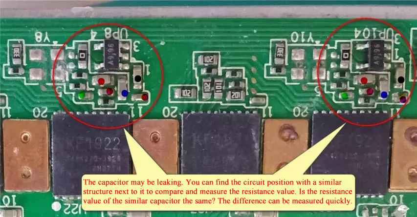
The related chips are often replaced. Since 3 chips on the same layer are connected in parallel, , May cause the signal to fail to pass, in addition, the current leakage of the capacitance of the current layer will also affect the normal operation of the chip. It is necessary to switch the multimeter to the resistance file for comparison and measurement.
3. The reset is normal, and the chip reading fails completely or partially
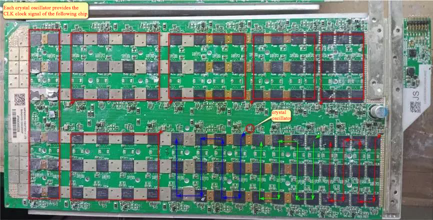
RST is normal, and the chip reading fails. At this time, it is necessary to measure whether the transmission of the CLK 0.9V signal from U1 →U105 is interrupted . If there is, repair the related chip and LDO circuit, check the CLK related chip, and the same layer will have an impact. If the CLK interrupt is at the crystal oscillator, the chips behind it cannot be read, and the crystal oscillator may be damaged.
At the same time, check whether the capacitor at the interruption point is leaking.
If the CLK signal is normal, the next step is to measure whether the 1.8V RXD signal transmission from U1 →U105 is interrupted . If there is an abnormality, check whether the chip is faulty, whether the LDO is normal, and measure the relevant layer capacitance whether there is electricity leakage.
If the RX measurement is no problem, then the measurement is from signal transmission of U105 →U1 is The 1.8V TXD; If it is interrupted, the TXD interruption may also be due to a defective chip, a defective LDO, and whether the relevant layer capacitance is leaking.
4. The detection of the whole board is mainly based on measuring the signal voltage, and at the same time supplemented by the method of measuring the resistance of the capacitor for maintenance.
5. When some hashrate boards started testing, it was found that the power current speed increased rapidly, and the hashrate boards quickly heated up. This is caused by when an abnormal signal voltage causes the chip to start working, the signal needs to be measured quickly during maintenance, and it needs to be blown cold after heating. Only then can be tested again.
6. Boards with unbalanced layer voltages. However, the signal transmission cannot be restored by repairing and replacing the chip. For example, some layer voltages are close to 0.5V, Some layers are only 0.2V. When the board temperature is lower, the voltage of each layer is measured as a mark.
The lower layer swaps a chip to balance the layer voltages. If there are several unbalanced layers, you need to swap several layers, and the voltages are balanced. Fix the signal later.
7. Some chips cannot be read in the software test, and the first chip may be reported as bad. If there is a crystal oscillator next to it, There may be a problem with the crystal oscillator.
8. LDO output pin 5 does not have 1.8V, check if the input pin 1 voltage is sufficient, if the input is not normal, look for the relevant circuit in front of the input, if the input is normal, the output is not normal, replace the LDO chip, if the replacement of the LDO is still abnormal, consider Whether the current layer chip he is powering is bad and pulls down the voltage, and the power next to the LDO is the capacity leaking?