


Ⅰ. Appearance visual inspection
For a failed control board, the first thing to check is its appearance. The visual fault detection sequence is as follows:
1. Connector damaged
These include 22-pin connector to connect the control board to the miner, 14-pin connector to connect the control board to the miner power supply, and 6-pin connector to connect the control board to the fan.
The inspection method is mainly to visually observe whether the plastic shell of the connector interface is cracked, whether the connector socket is deformed, etc. If there is any abnormality, replace the corresponding material.
2. Button damaged
The inspection method is mainly to visually observe whether there is rust or cracks on the surface of the button. Observe whether the button returns to its original position after being pressed. Press the button to feel whether the physical elasticity is normal.
If there is any abnormality in the above operation, please replace the button.
3. The Ethernet socket or Ethernet network transformer is damaged
The inspection method is mainly to visually observe whether the Ethernet connector is deformed, whether the Ethernet connector pins are deformed, whether the network transformer pad is raised and whether the network transformer body is damaged.
If there is any deviation, please replace it with suitable material. If some boards have their transformer gaskets lifting and falling off, that board will be discarded without further repair.
4. Inductor damaged
The inspection method is mainly to visually observe whether the inductor pad is raised, whether the inductor is damaged, etc. If there is any abnormality, replace the inductor material. If some of the inductor traces rise and fall, the board will be scrapped without further repair.
5. Electrolytic capacitor is damaged
The inspection method is to visually observe whether the shell of the electrolytic capacitor is cracked or whether the top of the electrolytic capacitor is punctured. If there is any abnormality, the electrolytic capacitor should be replaced.
6. LED light damaged
The inspection method is to visually observe whether the LED lamp body is damaged. If there is any abnormality, please replace the LED light material.
7. Scratches on the circuit board
The inspection method is to manually observe with the naked eye whether there are scratches on the front and back of the circuit board. If there are scratches that cause circuit traces to be cut or pads to be scratched, the board will not function properly.
Ⅱ. Resistance measurement
After completing the visual inspection, start measuring the resistance. The purpose of measuring resistance is to find out whether there is a short-circuited module on the board that needs to be repaired and to avoid the phenomenon of high currents burning the board or test equipment during a short circuit. When measuring resistance, the specific steps are as follows:
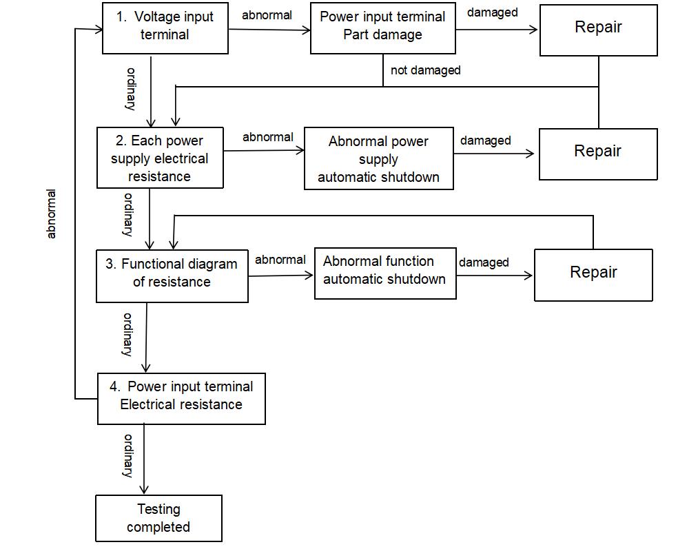
1. The resistance of the power input terminal is normal
Measure the resistance of the row connector of the power input terminal, or the resistance of the positive electrode of the electrolytic capacitor at the power input terminal relative to the ground.
Taking CB2_V10 as an example, check whether the resistance to ground matches any position in ①, ②, and ③ in the figure below.
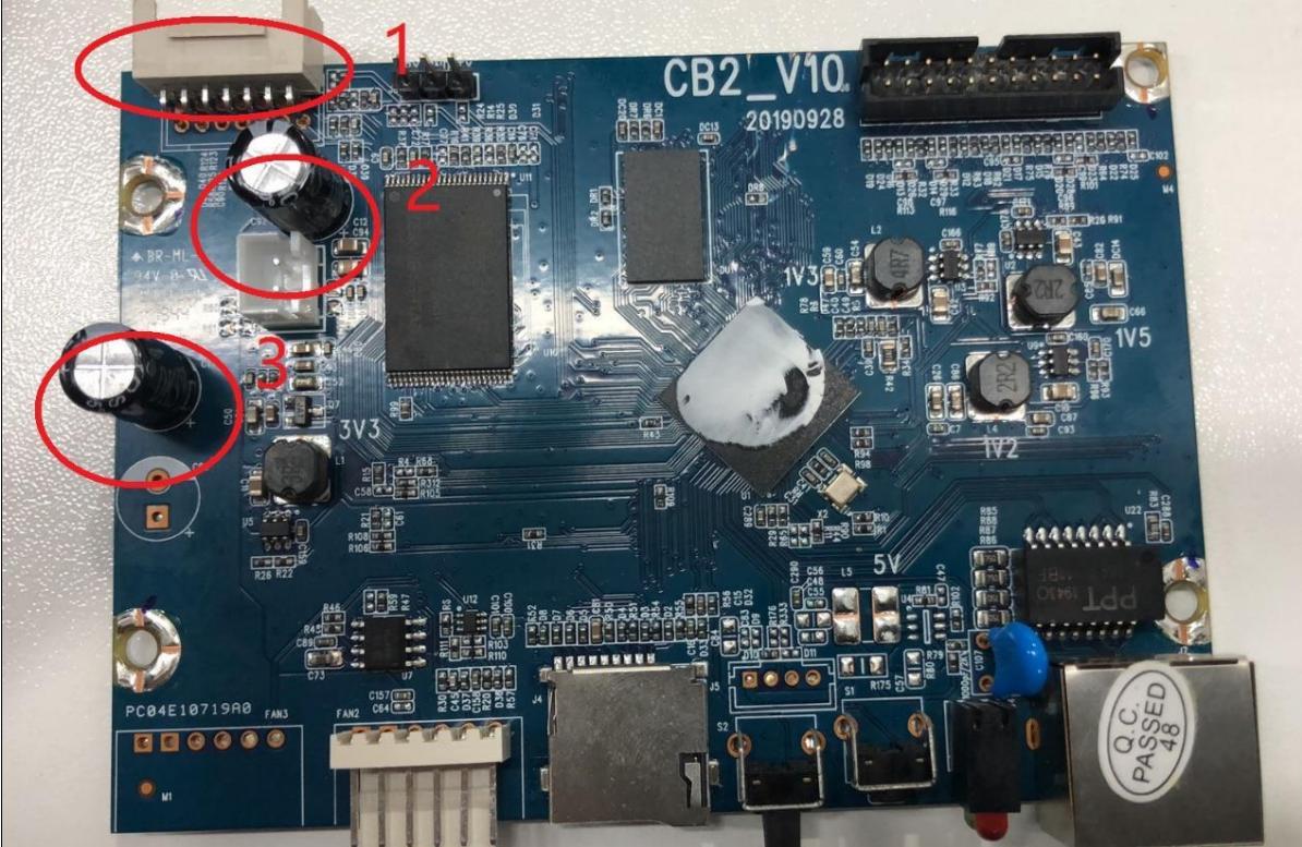
Note:
(1) Measure the normal value through several normal test boards to obtain the reference range.
(2) In the above figure, ① is the power input terminal socket, ② and ③ are the electrolytic capacitors on the power input terminal.
If the resistance at the power input terminal is normal, proceed to the next step: check the resistance of each power supply.
If an exception occurs, do the following:
A. Gradually remove material devices associated with the anomalous point. If the resistance becomes normal after removing a specific control board component, stop the removal. Go to the next step: Check the resistance of each power converter.
B. After removing all materials and devices related to the power input terminal, if the resistance is still not within the standard range, proceed to the following steps: test the resistance of each power supply.
2. The load resistance of each power supply is normal
Measurement resistance of each power circuit is normal.
For CB2_V10 example, check whether the grounding resistance at any position ①, ②, ③, ④ as shown below is normal.
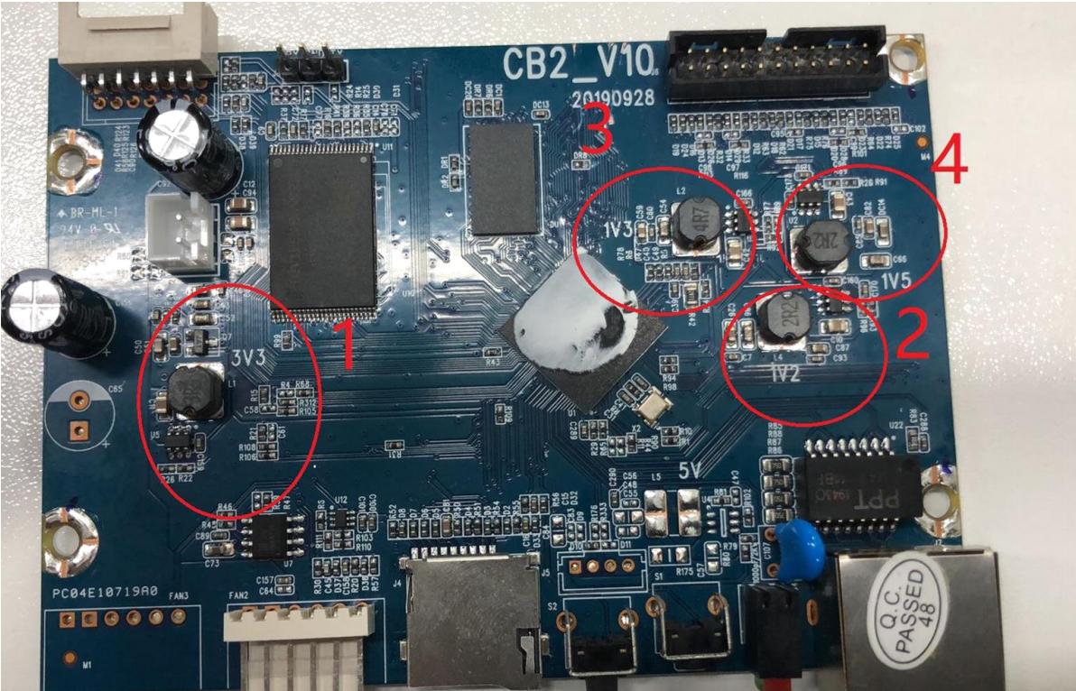
Note:
(1) For normal values, take some good board measurement reference ranges.
(2) ①, ②, ③ and ④ in the above figure are the power circuits of 3.3V, 1.2V, 1.3V and 1.5V respectively. The power circuit for other models of control boards can be found via the silk screen printing on the board.
If the resistance of each power circuit is normal, proceed to the next step: check the resistance of the functional circuit.
If abnormal, please perform the following operations:
A. Gradually remove materials and devices associated with abnormal points. If the impedance of the power circuit becomes normal after removing a certain device, stop the removal and proceed to test the impedance of the next power circuit.
B. Until the impedance of all power circuits is normal, proceed to the next step: check the resistance of the functional circuit.
C. When all materials and components related to the power circuit have been removed and the resistance is still abnormal, proceed to the next step: check the resistance of the functional circuit.
3. Resistance of functional circuit is normal
Check whether the resistance of each functional circuit is normal.
For example, CB2_V10 is shown as ①, ②, ③, ④, ⑤, ⑥, ⑦, ⑧, and ⑨ in the figure. Check whether the grounding resistance on the front and back of the board is normal.
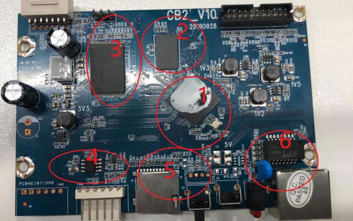
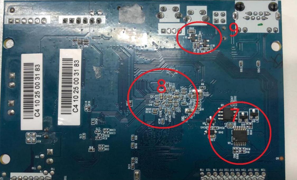
Note:
(1) Normal value, take several normal boards to measure the reference range;
(2) Figures ①, ②, ③... show the main control circuit, DDR circuit, Nand Flash circuit, etc. respectively. The functional circuits of other types of control boards can be distinguished according to their positions on the board;
If the resistance of each functional circuit is normal, the resistance test is completed.
If abnormal, please perform the following operations:
A. Gradually remove material devices related to abnormal points. If the resistance becomes normal after disassembling the functional circuit to a specific device, stop the disassembly and proceed to the next functional circuit resistance test.
B. Until the resistance of all functional circuits is normal, the resistance test is completed.
After completing the resistance test, recheck the resistance of the power input terminals. If it is also normal, weld the previously removed material. Then enter the voltage test (when re-soldering, make sure the material is good and can be reused).
If the resistance value at the power input terminal is retested and still does not meet the standard, it means there was something missing in the last test. Repeat the above process until the measured resistance value is normal. After the resistance test is normal, re-solder the removed materials and then perform voltage test.
Ⅲ. Voltage measurement
After completing the appearance and resistance inspection, start measuring the voltage. When measuring voltage, the specific steps are as follows:
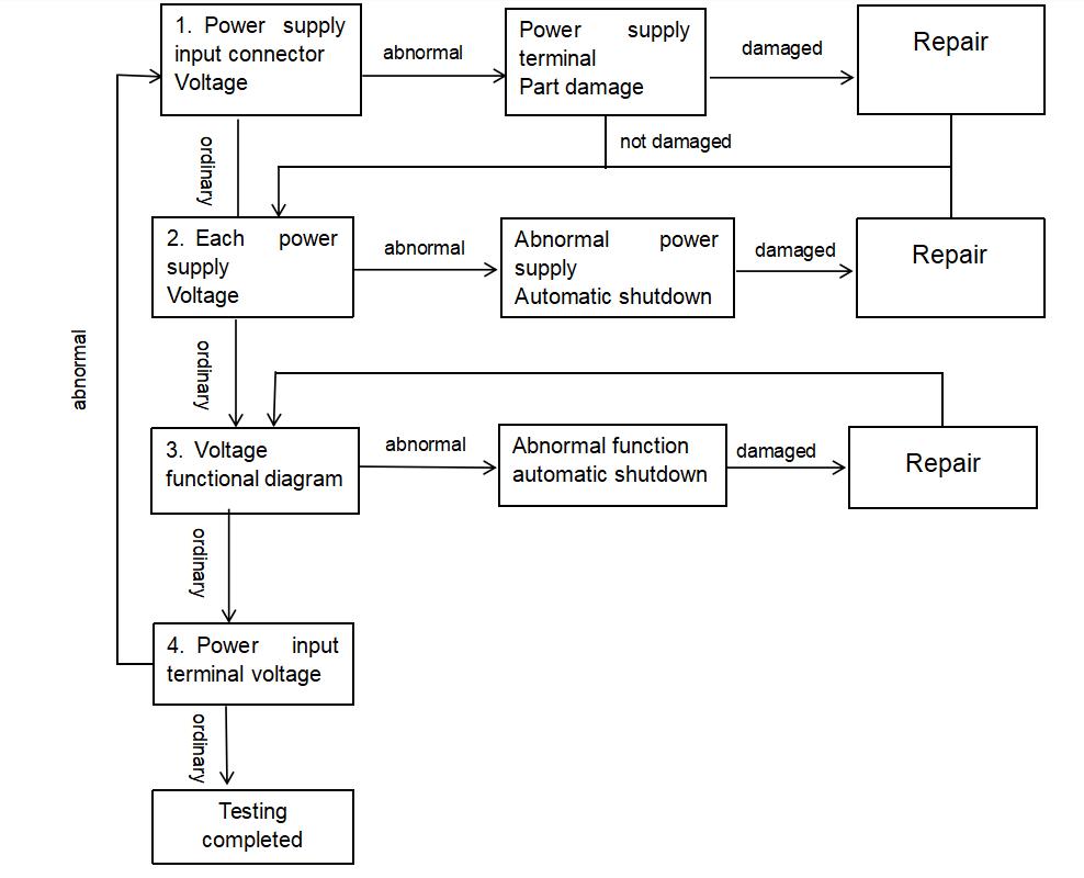
1. The power input terminal voltage is normal
Check the voltage of the row connector of the power input terminal, or whether the positive electrode of the electrolytic capacitor on the power input terminal is properly grounded. Taking CB2_V10 as an example, check whether the voltage at any position in ①, ②, and ③ in the figure below is normal.
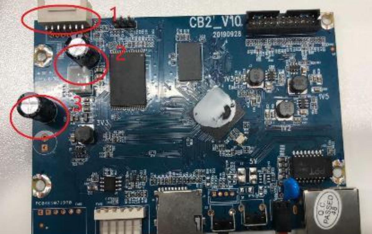
Note:
(1) Use several good reference boards to measure normal values and obtain the reference range.
(2) In the above figure, ① represents the power input terminal socket, ② and ③ are the electrolytic capacitors of the power input terminal. If the voltage at the input terminal is normal, please proceed to the following test steps: Check the supply voltage of each power supply.
If abnormal, please perform the following operations:
A. Gradually replace the materials and devices related to the abnormal point. If the voltage is normal after removing a certain component, stop the removal and proceed to the following steps: Check the supply voltage of each power supply.
B. After removing all materials and devices related to the abnormal location, if the voltage is still abnormal, proceed with the following steps: Check the supply voltage of each power supply.
2. Each power supply voltage is normal
Check whether each power supply voltage is normal. Taking CB2_V10 as an example, check whether the voltages at ①, ②, ③, and ④ in the picture are normal.
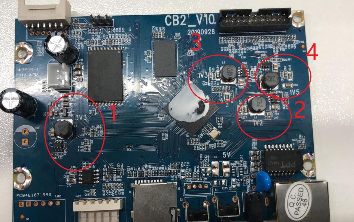
Note:
(1) Use several good reference boards to measure the normal values to get the reference range.
(2) ①, ②, ③, and ④ in the above picture are the power circuits of 3.3V, 1.2V, 1.3V, and 1.5V respectively. The power circuits of other types of control boards can be found through the silkscreen on the board.
(3) Voltage measurement can measure the voltage across the capacitor or the voltage difference between the inductor and ground;
If the supply voltage of each power supply is normal, perform the following test steps: Check the functional circuit voltage.
If an exception occurs, do the following:
A. Gradually replace the materials and devices related to the abnormal point. If the voltage of a power circuit becomes normal after replacing a device, stop replacing it and proceed to the next power supply voltage test.
B. After the power supply voltage of each circuit is normal, please proceed to the following steps: Check the functional circuit voltage.
C. After replacing all materials and devices related to the power circuit, if the voltage is still abnormal, proceed with the following steps: Check the voltage of the functional circuit.
3. Functional circuit voltage is normal
Check whether the voltage of each functional circuit is normal. Taking CB2_V10 as an example, check whether the power supply voltage at the front and back of the board is normal, as shown in ①, ②, ③, ④, ⑤, ⑥, ⑦, ⑧, ⑨ in the figure.
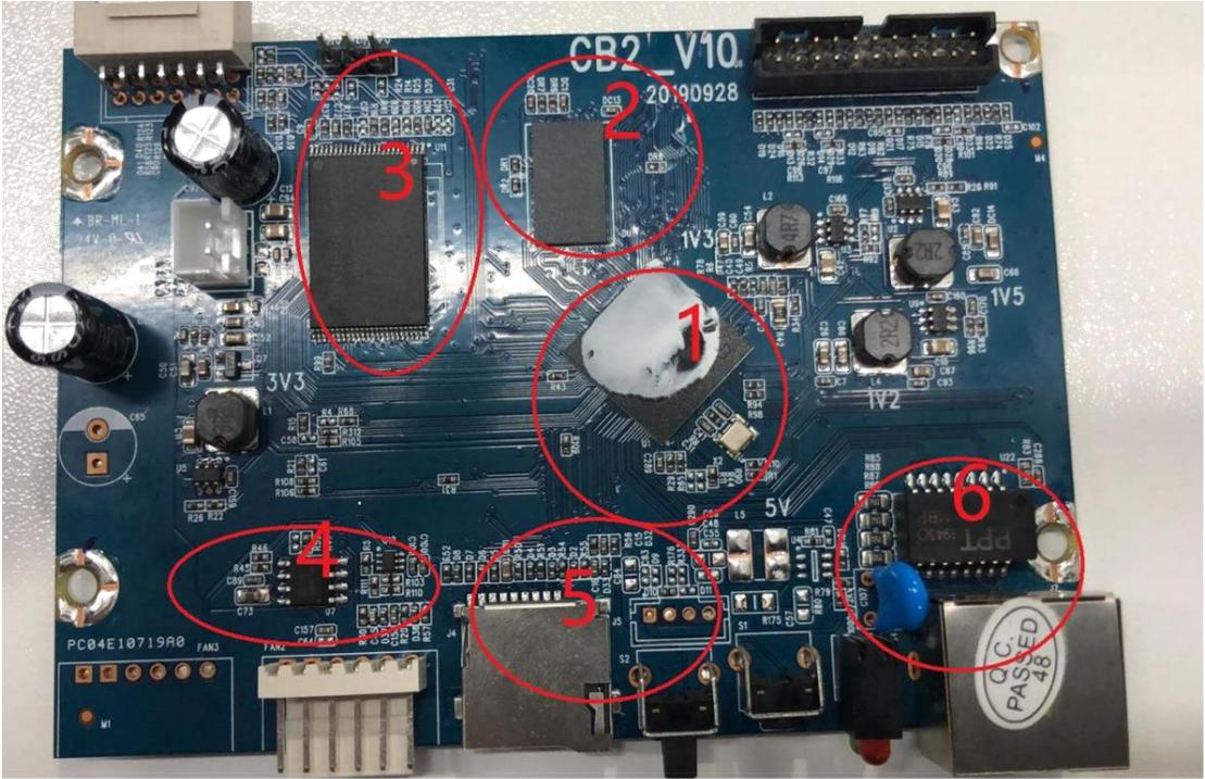
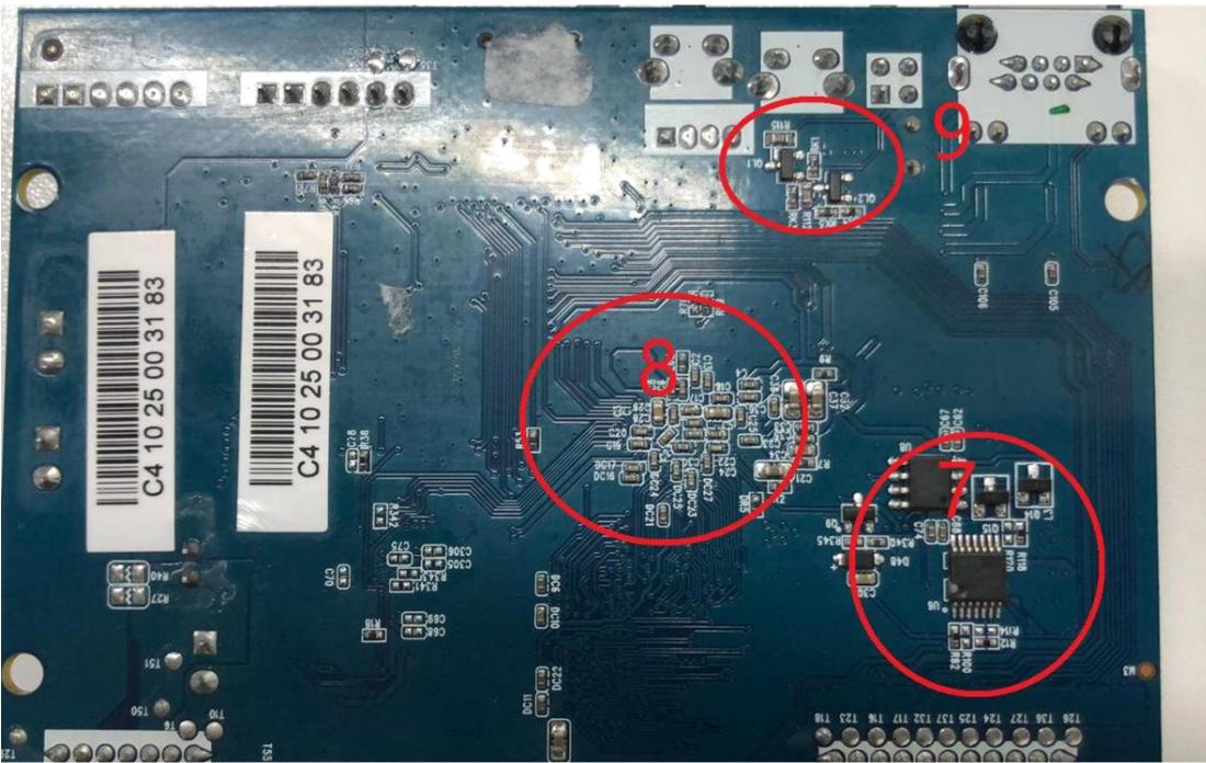
Note:
(1) Use a good reference plate to measure the normal value to get the reference range.
(2) ①, ②, ③... in the figure are the main control circuit, DDR circuit, Nand Flash circuit, etc. The functional circuits of other models of control boards can be distinguished based on their location on the board.
(3) During measurement, check the voltage on the capacitor in this area:
If the voltage of each functional circuit is normal, the voltage test is completed.
If abnormal, please perform the following operations:
A. Gradually replace the materials and devices related to the abnormal point. If the voltage is normal after replacing with a certain device, stop replacing and enter the voltage test of the next functional circuit.
B. Until all functional circuit voltages are normal, the voltage test is completed.
After the voltage test is completed, recheck the power input voltage. If it is also normal, it means that the voltage test is completed, and then enter the test firmware check.
If the voltage at the power input terminal is still abnormal after retesting, it means that there was something missing in the previous test. Repeat the above process until the voltage test is normal, and then perform the test firmware verification.
Ⅳ. Test firmware
After the voltage test is completed, enter the test link to check the firmware. If a test failure occurs during a test, find the specific function diagram using the failure information and replace the material of the specific function diagram.
1. Test firmware update
The test must first perform test programming of the test firmware update. If the programming update is successful, the internal module test is performed. If the programming update is not successful, it needs to be repaired by gradually replacing the circuit materials related to the main control element, DDR chip, and Nand Flash chip module until the programming update is successful. If it's a card update, you need to check the card module circuit, and if it's an OTA update, you need to check the Ethernet port circuit, etc.
2. Internal module test
After successful programming and updating, after power-on, the module's internal test will be performed, which will cover CPU, DDR, NAND, network, and other functions. If the test passes, move on to the I/O test.
If the test fails, you need to exclude specific modules according to the error message.
If a message appears that the DDR test fails, you need to simultaneously eliminate the circuit materials related to the main control and the DDR chip and so on.
3. I/O test
After successfully testing the internal module, go to the I/O testing link. The I/O test should plan the I/O under test in advance and reflect the corresponding test cases in the test firmware. In the test case, the expected value output of the required test I/O is measured by an external multimeter to check whether the I/O under test is working normally. If you find that any output is not as expected, the materials and basic controls on the I/O path must be addressed to resolve the problem.
If the above tests are passed, the board repair is complete.