

How to repair Bluestar L1 hash board?
Ⅰ. Principle Overview
1. Bluestar L1 hash board structure:
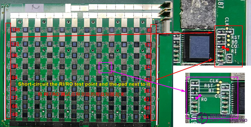
The hash board (No. L0010-B) consists of 108 chips divided into 18 domains, each containing 6 ASIC chips. The operating voltage of the ASIC chip is 0.68V. The yellow boxes identify chips in the same domain; the chip numbers are shown in the figure.
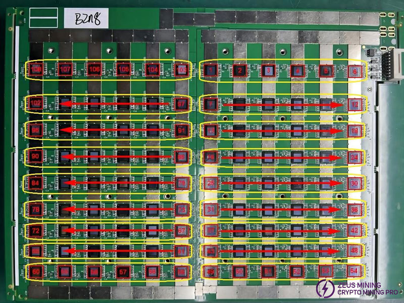
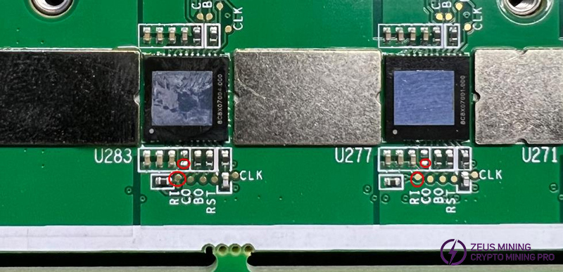
Note: near the edge of the board is the last chip of each domain, as shown in the figure, short-circuit the test point and the pad.

The 18th, 17th, 16th, and 15th domains (4 groups in total) are powered by 18V output by the boost circuit to power the LDO chip, and then the LDO chip outputs 1.8V; Domain 14 - Domain 1 is provided with 1.8V by VDD through the LDO chip. All 0.8V is provided by the 1.8V of this domain through the LDO output.

Each time a domain is stepped back, its voltage decreases by 0.68V.
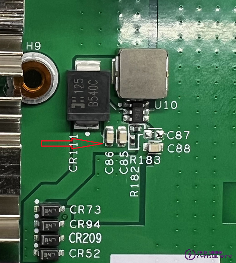
Ⅱ. Boost circuit of hash board: 12V to 18V
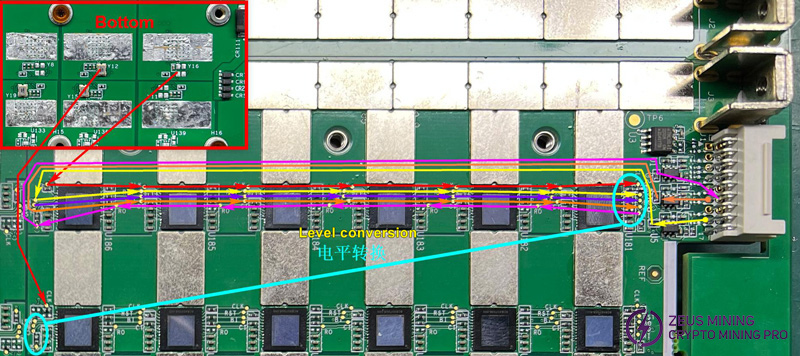
Ⅲ. ASIC chip signal direction
1. Red - CLK signal flow: It is generated by the crystal oscillator of each domain on the Bottom side, then transmitted from chip 01 to chip 06 (in the second domain, it is generated by the corresponding crystal oscillator and is transmitted from chip 07 to chip 14, and the same applies to other domains), with a voltage of about 0.8V-1.3V;
2. Orange - TX (CI, CO) signal flow: Entering from IO interface J1 (3.3V), after passing through level conversion IC U2, it is transmitted from chip 01 to chip 06 in the first domain and then transmitted to chips 07-14 in the second domain through the level conversion chip, and so on until chip 108; the voltage is 0V when the IO cable is not plugged in, and the voltage is 1.8V when powered on;
3. Pink - RX (RI, RO) signal flow: sent from chip 108 to chip 103 in the same domain, then to chip 102-97 in the previous domain through level conversion, and so on until chip 1, after level conversion IC U1, enter IO interface J1 (3.3V); the voltage is 0V when the IO cable is not plugged in, and the voltage is 1.8V when powered on;
4. Purple - BO (BI, BO) signal flow: from chip 01 to chip 06 to complete the transmission of the first domain, then to chip 07-14 in the second domain through level conversion, and so on until chip 108; the multimeter measured 0V;
5. Yellow - RST signal flow: from IO cable port J1 (3.3V), after level conversion IC U5, from chip 01 to chip 06 to complete the transmission of the first domain, and then to chip 07-14 in the 2nd domain through level conversion, and so on until 108 chip; the voltage is 0V when the IO cable is not plugged in, and the voltage is 1.8V when powered on.
Schematic diagram of level conversion circuit:
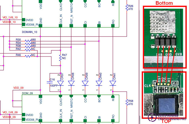
During the repair process, we can use a multimeter to check whether the diode is normal without removing the small heat sink on the back of the hash board. Put the positive pole of the multimeter on the pin of the diode on the bottom side near the board and the negative pole on the test point next to the chip. Normally, it is about 0.5V.
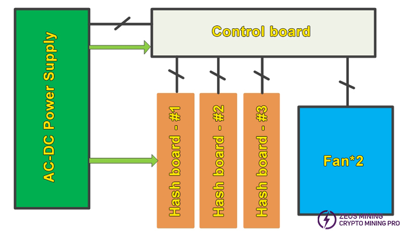
IV. Overall architecture
The overall architecture consists of 3 hash boards, 1 control board, 1 power supply, and 2 cooling fans.
Ⅴ. Common faulty phenomena and troubleshooting steps of hash board
1. General inspection
① Perform appearance inspection on all faulty boards before repair, and make records and take photos;
② Measure the resistance of the input voltage terminal. The normal range is 10-20Ω;
③ Measure the impedance of the large heat sink on the front side and the small heat sink on the back side, which should be an open-circuit, and the impedance should be greater than 600K;
④ Power on for testing, pay attention to the polarity, and do not reverse it;
⑤ Power on and test the input voltage, boost circuit voltage (18.5V), 1.8V/0.8V voltage of each domain;
⑥ Use a multimeter to test the series signal circuit voltage of each domain: CLK (0.8V~1.3V), RST (1.8V), BI (0~0.2V), CI/CO (1.8V), RI/RO (1.8V).
2. Summary of faults during the PT1 test
2.1. Incomplete ASIC chips (108 chips cannot be found)
108 chips cannot be found during PT1 test, and the number of chips returned is generally 0 or other numbers (less than 108).
Detection method:
Determine the actual number of chips through the RI / RO signal circuit, short-circuit the RI / RO and the pads next to it, and the number of chips at the corresponding position should be found in the PT1 test accordingly. As shown in the figure, the RO signal of chip No. 20 is short-circuited, so 20 chips should be found. By changing the number of chips actually added to the series signal, the problematic chip is found.
2.2. The number of chips is a multiple of 6, such as 24, 78, etc.
This is a special case of the second type of insufficient chip number. It is very likely that the diode of the level conversion circuit is abnormal.
Measure the conduction voltage of the diode and determine whether it is normal.
The multimeter is set to the diode position, and the measured voltage is about 0.5V.

2.3. No voltage was detected during the PT1 test
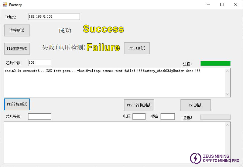
Check whether the U4 chip is soldered properly or replace the U4 chip.
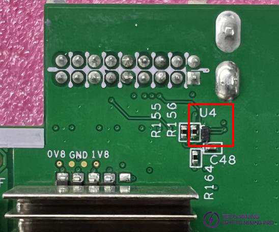
3. Summary of PT2 test process problems
PT2 test failed, extract the test log from the test interface.
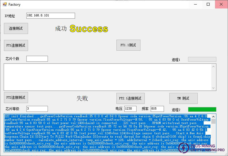
According to the test log, there are mainly two situations:
① Each chip has nonce, but the number of individual chips is 0 or very small.
The number of nonce for a normal chip is generally around 48.
Find the following fields from the log file. This part is basically around 48 in normal situations. Find the position where the data is very different.
Judge the chip by position. The number in the log starts from 0. Level 0 is the first level chip on the board.
As shown below, the corresponding chips are No. 29 and No. 45:
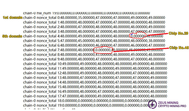
After replacing chips 29 and 45, the test passed.
② The first chip has a lot of nonce, but the number of other chips is 0, or the number is very small. As shown in the following figure:
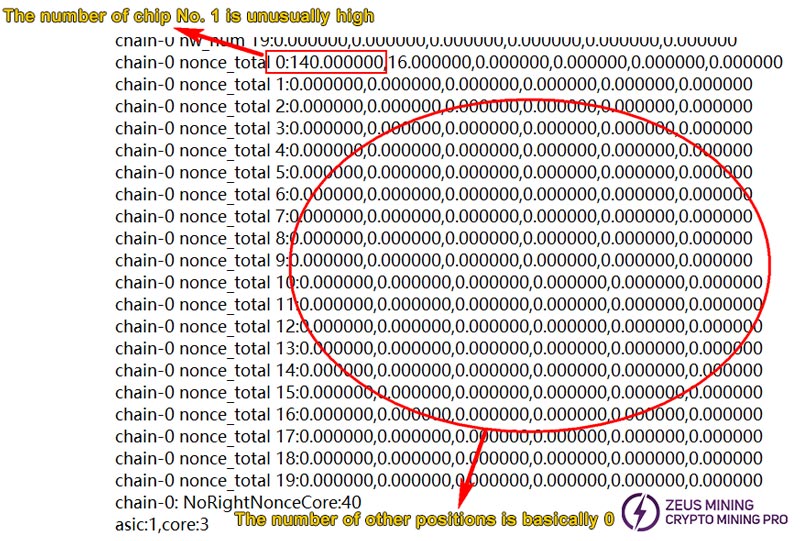
At this point, we perform the TM test.
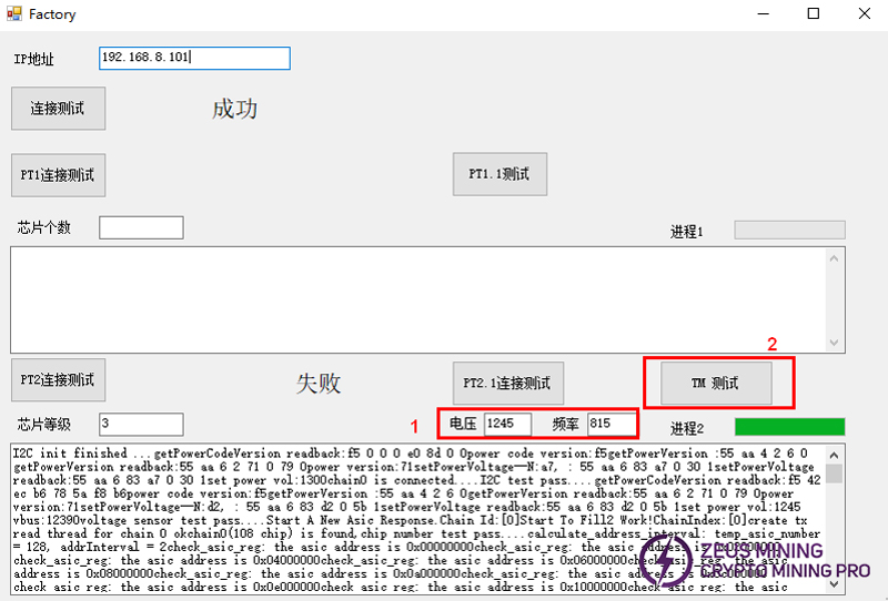
The test results are as follows:
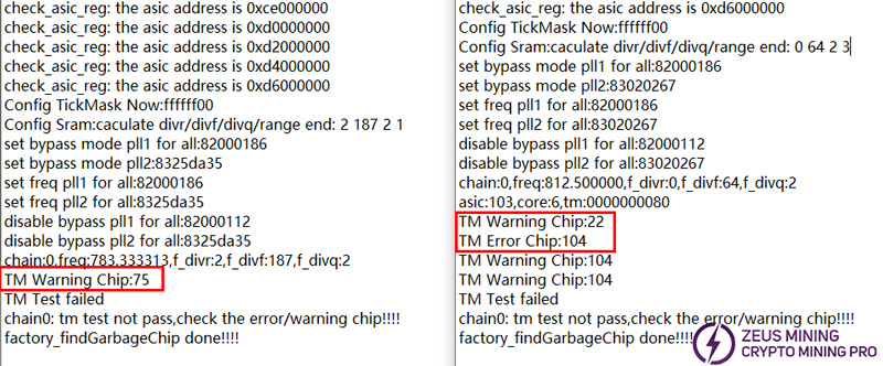
Find the chip numbers corresponding to the TM Warning Chip and TM Error Chip and then replace them.
After completion, re-perform the TM test, and the display level is 1. Note that this only means the repair is successful and the PT2 test is still required.
After successful repair, re-perform the PT2 connection test to calibrate the board level.
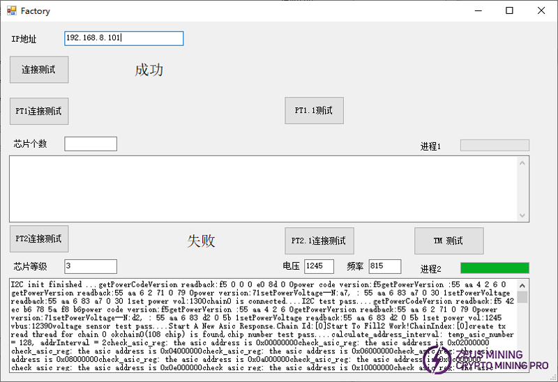
4. Use of the test tool:
(1) Double-click to run the new test tool. We need to enter the password: ltc@dog.
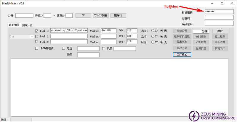
(2) During maintenance, the TM test is mainly performed.
