


Ⅰ. Purpose
This guideline is aimed at the operation guidance of welding and component replacement in the process of repairing defective products by maintenance personnel, so as to effectively ensure the quality of maintenance. Organized and shared E12 hash board repair tutorial by ZEUS MINING .
Ⅱ. Scope of application
Applicable to the entire repair process for E12 miners.
Ⅲ. Tools and Equipment
1. Soldering iron
2. Heat gun
3. Tin wire
4. Washing water
5. Anti-static brush
6. Multimeter
7. Soldering Station
8. Thermal grease (used to coat the hash board heat sink)
9. Drying oven (for baking chips) etc.
Ⅳ. Operation steps
1. Repair equipment
(1) Before maintenance, it is necessary to check the soldering iron head, electrostatic wristband, air gun, etc. to ensure that the equipment can work normally and that the ESD protection meets the quality requirements.
(2) The welding temperature range of the electric soldering iron is 330℃~390℃, and the welding duration is less than 5s.
(3) The maximum temperature range of the hot air gun is 390℃±30℃, and the wind speed is controlled within 6 gears.
(4) Wear an electrostatic wristband during maintenance.
(5) After maintenance and disassembly, it needs to be repainted with thermal grease and then assembled.
2. Instructions for maintenance operation
(1) Repair of bad appearance of veneer
Repair welding: When there is less tin in the solder joint, empty soldering, or virtual soldering, it is necessary to add tin to the solder joint to make up for tin.
Removal of tin: When the solder joints are over-tin or short-circuited, the excess tin needs to be removed.
Soldering quality: Check whether the PCBA board has bad phenomena such as tombstone, offset, reverse sticking, reverse and repair it. When a solder joint has defects such as poor dip soldering and particles, it is necessary to use a hot air gun or an electric soldering iron to repair the corresponding defective components. Check whether there are missing parts and missing parts. When welding materials, it is necessary to find the materials in the corresponding positions according to the product component model to ensure that the replacement materials are qualified products. When replacing materials, pay attention to the direction of the components and confirm the appearance to ensure the welding quality.
(2) Repair of bad single board function
According to the bad phenomenon, analyze the fault line of the circuit and related parts that realize the function. Combined with the schematic diagram, use a multimeter to measure the continuity of the circuit, whether there is a short circuit, open circuit, welding quality, etc.;
If there is any abnormality in the program during the maintenance process, please use the relevant software to re-burn or download it.
(3) Maintenance welding method
Soldering with electric soldering iron: Use an electric soldering iron to remove tin and clean the pad. After confirming that the chip is placed in the correct direction, carefully align the chip and place it on the hash board pad with tweezers. Pay attention to the regularity of the chip pins. Dip a small amount of solder on the tip of the soldering iron, press down on the chip that has been aligned with a tool, and solder the pins on two opposite corners, so that the chip is fixed and cannot move, and check the position of the chip again after soldering the opposite corners Is it aligned. Otherwise, it needs to be adjusted or removed and re-aligned on the board. When you start soldering all the pins, you should add solder to the tip of the iron and apply solder paste to all the pins to keep the pins wet. Touch the end of each pin with the tip of a soldering iron until you see solder flowing into the pin. When soldering, keep the tip of the soldering iron in parallel with the pins to be soldered, and easily hold the tin wire to prevent solder bridge short-circuit or pin deformation due to excessive soldering or uneven force.
Hot air gun soldering: You can apply an appropriate amount of flux to the pad and use a hot air gun to heat the tin and then clean the pad. After confirming that the chip is placed in the correct direction, use tweezers to carefully align the chip and place it on the single board pad. Pay attention to the regularity of the chip pins. Use a hot air gun to fix the diagonal pins first, apply an appropriate amount of flux, and adjust the chip welding direction in real time during the heating process to ensure that the pads are aligned and the welding reliability is good.
After soldering, touch the pins with tweezers to check for poor soldering. Use an electrostatic brush to thoroughly clean the flux in the direction of the pins when finished, making sure there is no flux around the chip.
3. Welding precautions
(1) Before welding, it is necessary to protect the surrounding components that are easily affected by heat with high temperature tape.
(2) Pay attention to the welding quality, and reprocess the solder joints that do not meet the requirements.
(3) For disassembly/soldering, a hot air gun can be used with a soldering iron. When handling the air gun, handle it with care to avoid damage to the heating element of the equipment.
(4) Do not place other items in the heat gun placement area, so as not to scald the items with strong heat.
Ⅴ. Repair Steps
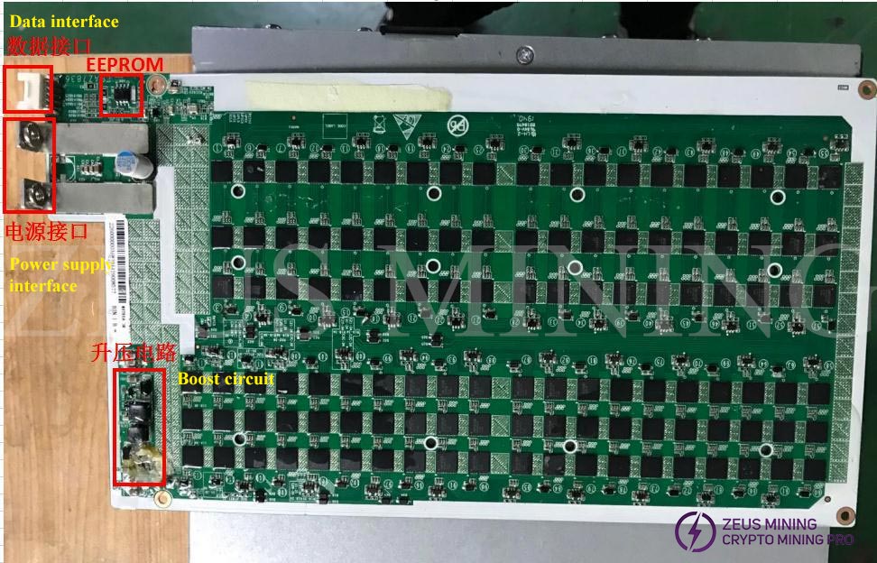
1. Hash board component structure
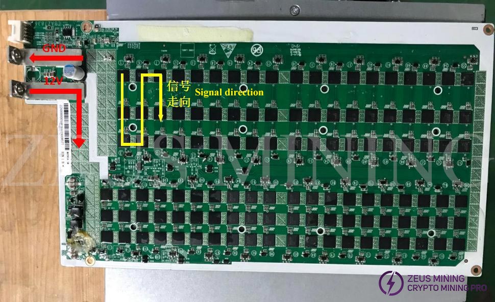
2. Hash board signal flow diagram
3. Analysis of hash board
Use the special E12 tooling board to running software (scan the chip ID, PLL signal, the hash board is a single channel of 117 chips and can scan all the chips, and can lock the PLL of each chip)
(1) Brief description of the installation and use of the tooling board running software running
① Purchase the fabricated tooling board 4303 (supporting the maintenance tooling running software Ebangrunning_V1.3.rar);
② Unzip the running tooling board software  to the root directory of the D drive;
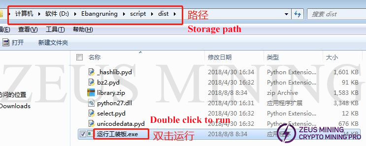
③ Enter the dist directory in this folder, find the run icon and send the shortcut to the desktop, and run it; (see the figure below for the operation)
(2) Precautions for installation and use of tooling
① This software can only be used in the root directory of the D drive;
② Do not manually open the tftpd32/CRT software before using the tooling;
③ If the use is not in the same network segment, you need to add the same network segment in the ipv4 settings;
④ The CRT window may report an error when using it for the first time. You can double-click SecureCRT in the CRT folder to run it once and then close it to use it normally. If you are prompted to verify the serial code in the following window, follow the steps below;
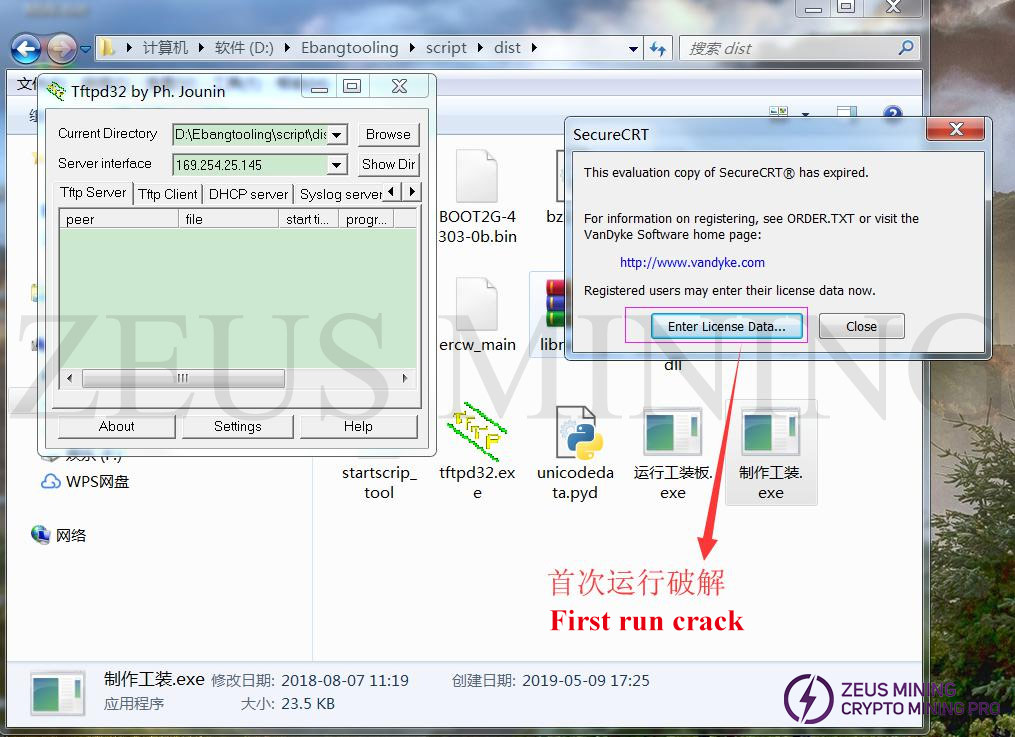
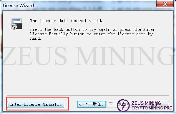
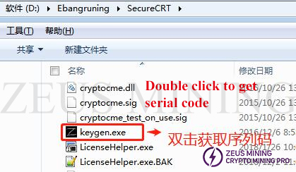
Open the marked file under the directory folder below to obtain the serial verification code;
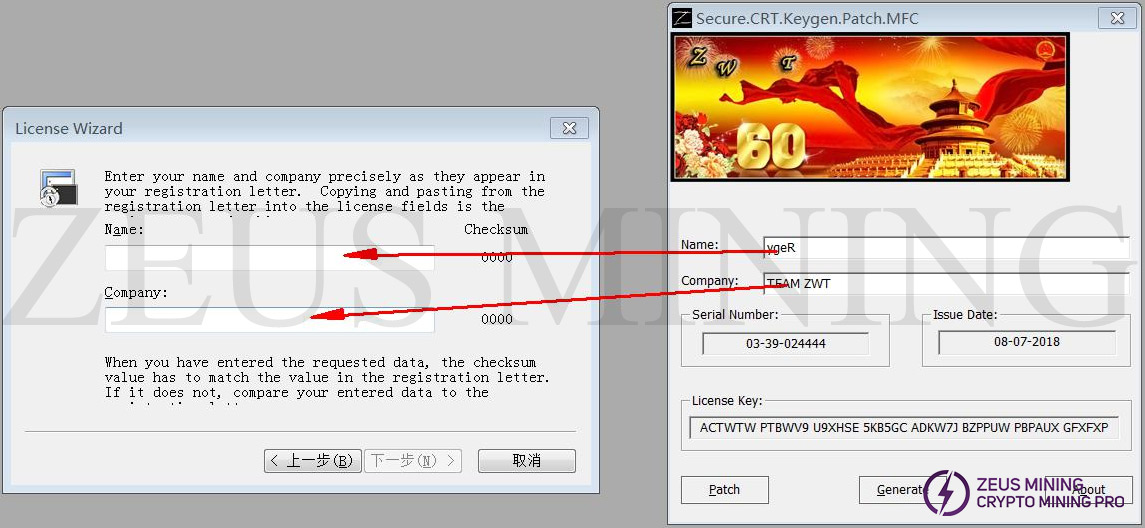
Fill in the parameters of the following two interfaces one by one.
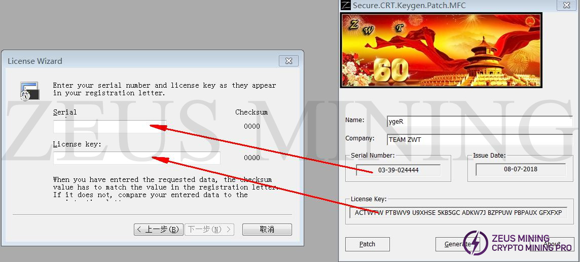
(3) Tooling use steps:
① First power up the tooling board and connect the network cable directly to the computer;
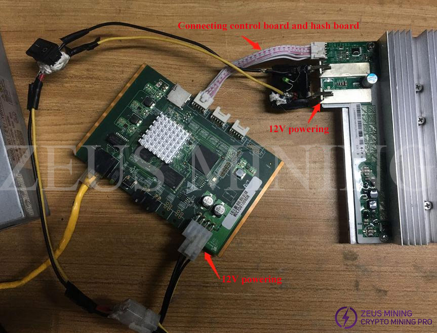
②Double-click  to pop out the window, enter the software version number corresponding to the miner, and enter the control board IP to enter the test page. Then connect it to the hash board cable. When the ID scan test is performed, connect the power supply to the hash board.
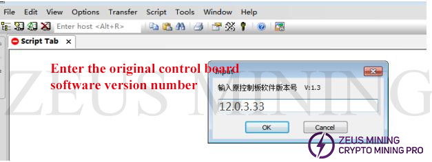
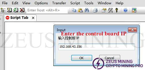
③You can choose to scan the ID and PLL test of the hash board;
Scan ID to select 0

Scan PLL to select 1

④Possible misprinting situation:
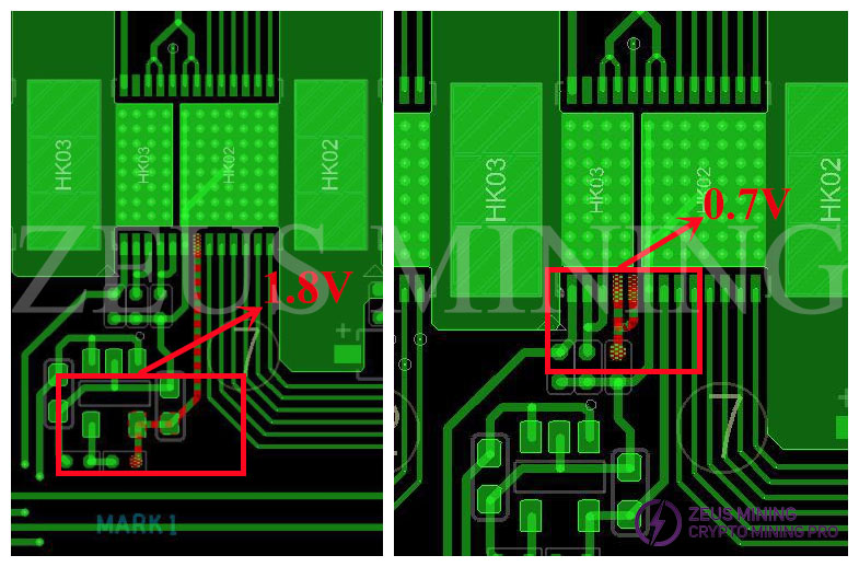
a) board 0 chip 1 id not found
Testing failed -----------
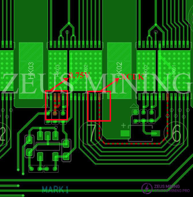
This means that the chip ID is not found, and confirm whether the voltage of Chain 0 Chip 1 1.8V (pin 5 of LDO) and 0.75V (0.75 IO) are abnormal, as shown in the figure below:
b) Chip 1 pll unlock, stop loading !
Testing failed -----------
Indicates that the chip PLL is not locked. Confirm whether the voltage of the capacitor in the figure below of Chip 1 is 0.75V (pin 1 of LDO), and the average voltage of the XCLK clock signal is 0.9V, as shown in the figure below:
(4) Hash board failure measurement
① If the scanning chip ID cannot reach 117, remove the two small heat sinks, and measure whether the 1.8V and 0.75V powering scanned to the chip are normal;
a) 1.8V output is abnormal: Whether the input of LDO Pin1 is above 2.5V, and whether the output is shorted to ground.
b) 0.75V output is abnormal: 0.75V is the LDO output inside the hash chip, measure whether the input pin voltage is normal (1.2V-2V), and whether the input pin and output pin are short-circuited to ground.
c) For equipment equipped with heat sinks, it is necessary to consider whether there are foreign objects on the heat sink or protrusions on the heat sink, which may damage the device.
② If the powering voltage is normal for the hash board, we need to further troubleshoot the fault:
a) Measure whether the voltage or impedance of the communication line is normal, which can be compared with the data of the normal hash board. To measure the voltage of the communication line, power supply should be connected to the control board, and to measure the impedance, the power should be cut off and the control board should be unplugged.
b) Or measure the data with an oscilloscope. Use an oscilloscope to measure the chip's data. Assuming that the chip N is currently scanned, the measurement chip N sends the data of the chip N+1, and the measurement chip N+1 returns the data of the chip N. If the data of the chip N+1 sent by N cannot be measured, the N chip needs to be replaced; if the data returned by N+1 cannot be measured, the N+1 chip needs to be replaced; if there is no test condition, use a multimeter Measure the voltage and impedance, and replace the chip directly if it is normal.
③ Other possible situations that can be scanned by 117 chips: Make sure that the power input voltage of the maintenance test is greater than 12.6V (because it is an adjustable power supply).
Notice: After the hash board is repaired, repaint the thermal grease and assemble it into a complete miner to run hash power verification.
Ⅵ. Maintenance experience of common faults
1. The ID cannot be scanned, and the measurement finds that the 0.75V input and output of this domain are very low.
Solution: The fault point of this problem is not necessarily in this domain. From the domain where the ID cannot be scanned, go to the next 2 domains in order, test the 0.75V input voltage of these domains, and find the domain with the lowest input voltage. The 1.6V input pin of one chip in this domain is shorted to ground.
2. Many chips are unstable when scanning ID or PLL.
Solution: Check whether the 1.8V input and 0.75V input at the unstable place are abnormal. If the voltage is low, it may be caused by the low core voltage of several consecutive chips. It is necessary to switch the position of the chip with low core voltage and the chip with high core voltage until the 1.8V input is above 2.5V, and the 0.75V input is above 1.2V.
3. The last few domain clamp diodes are burned out.
Solution:
(1) Check and replace the burnt chip and diode first.
The main reason for the burnout during power-on measurement is that the 1.7V voltage of the last few domains are abnormal. If the voltage is lower than 1.2V, it is an abnormal fault, which will cause the CORE voltage to rise instantaneously and burn out the diode and the chip 0.75V LDO. Some chips are not completely damaged after being burned out, they can run in a short time, and they will be damaged again after a period of time. These chips need to be found out and replaced all at once.
Measurement methods:
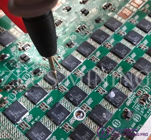
A. The last four domains can be directly measured, the multimeter is set to the diode gear, the red test lead is grounded, and measure the impedance at the filter capacitor of the 0.75V LDO input pin of the chip (as shown in the figure below), which is normally above 0.5 (different multimeters are different, and can measure the normal hash board for reference), if it is lower than 0.5, at least one of the 3 chips in this domain is abnormal, you need to remove one of them to measure, and measure the impedance of the remaining two chips on the hash board until all the bad chips are removed. Replace all chips (chips close to 1.8V LDO have a high probability of abnormality).
B. Since the powering of other domains is 12V and the impedance is very low, it cannot be measured directly. It is necessary to remove the chip near the 1.8V LDO and measure the removed chip and the rest chip of the domain on the hash board.
It is necessary to judge the penultimate 7th domain, and so on, until no chip is burned out in a certain domain.
Note: The performance of the replaced chip is as close as possible to the chip on the hash board (mainly the quiescent current is close).
(2) Adjust the diode (The adjusted version does not need to be adjusted again)
A. Replace the common diode G1M (3030500013) with bit numbers D19, D24, D32, D30 with the Schottky diode DS16W (3030200038)
B. Replace the Schottky diode DS16W (3030200038) of the bit number D20, D25 with the ordinary diode G1M (3030500013)
(3) Change the 1.8V LDO output voltage of the last four domains to increase the stability of the parallel diode circuit.
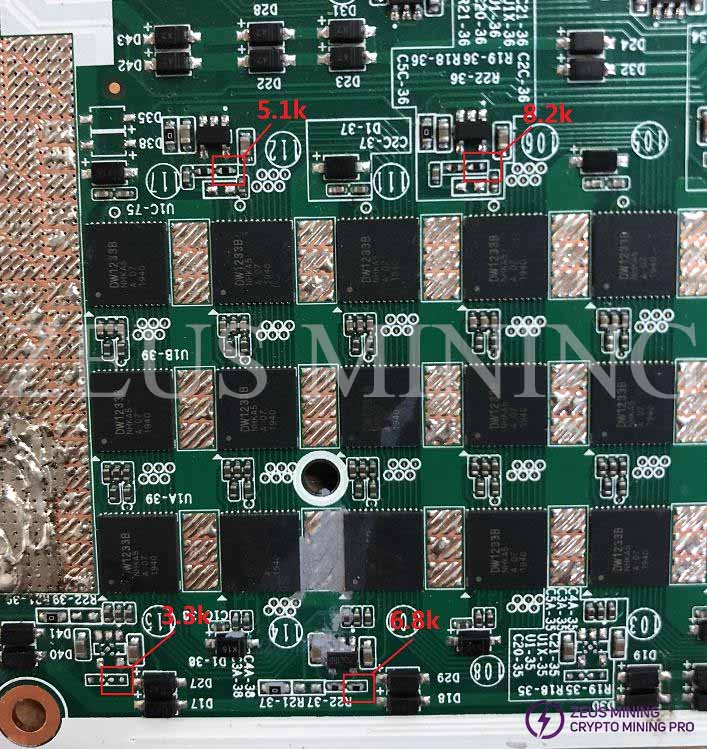
A. D17, D18, D20, D22, D23, D25 were originally two ordinary diodes G1M (3030500013) connected in parallel, after changing to three G1Ms in parallel, the order from the last domain is 1.4V, 1.5V, 1.6V, 1.7V. The specific operation method is to change the resistors of the last four domains, the resistance value is 3.3k, 5.1k, 6.8k, 8.2k from the last domain forward, as shown in the figure below. If it is a non-adjustable LDO, it is necessary to change the LDO of the last four domains to an adjustable LDO, and then add the feedback resistor.
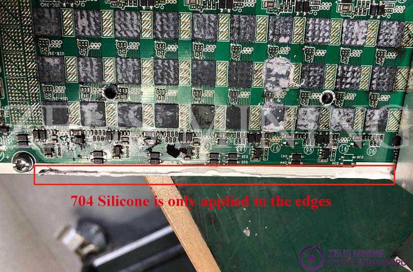
(4) Apply 704 Silicone Rubber
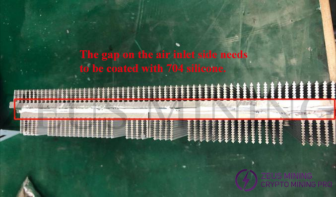
As shown in the figure below, apply 704 silica gel to the gap on the air inlet side of the repaired hash board to prevent dust from entering the hash board and accelerate the corrosion of components. The silica gel only needs to be applied to the gap.
(5) Paste the silicone gasket
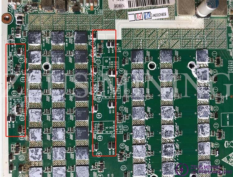
A. For the hash board of the BIN6 chip, paste a silicone gasket on the area shown in the figure below, and connect the diode with higher heat to the heat sink to accelerate heat dissipation.
B.D19, D21, D24 were originally two Schottky diodes DS16W (3030200038) in parallel, change to three DS16Ws in parallel. For other BIN chip hash boards, you only need to stick the silicone sheet on the burned-out diode, or you can choose to cover it all.
Note: The silicone pad is thicker and will expand under pressure. It should be noted that when the heat sink is pressed, the silicone pad will not be squeezed onto the ASIC chip.
(6) Increase the resistance and capacitance (the adjusted version does not need to be adjusted)
A. Bit numbers CB1, RB1 need to add a 220nF capacitor (3080105224003) and a 1M resistor (30701051004001).
(7) Apply coating glue and add windshield foam
Note: If the hash board has been coated with glue, it does not need to be brushed again; the heat sink of the old version does not need to be pasted with foam.
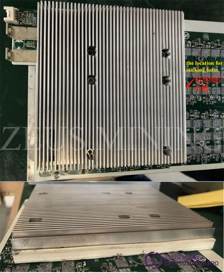
Purpose: Apply coating glue to prevent sticky ash from being corroded by moisture; after the new version of the small radiator is assembled, the gap is large, and it is necessary to add wind-blocking foam on the small radiator to prevent dust accumulation and corrosion of the power board. The old version of the small radiator has a small gap and does not need to be pasted.
Operate steps:
① Use an oil paintbrush or a soft brush to apply the coating glue on the hash board, in the three areas shown in the figure below.
Note: Do not paint on the ASIC chip.

② When installing the heat sink, you need to stick foam on the side of the upper heat sink first, and then install the heat sink. (As shown below):
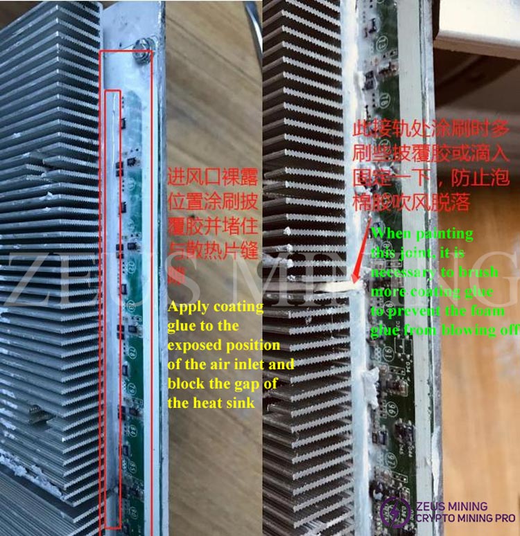
③After the heat sink is installed, the exposed part of the air inlet hash board should be coated with glue and the gap of the heat sink should be blocked; (see the figure below)
Attention: During the brushing process, it is necessary to drip coating glue into the rails of the heat sink for reinforcement, which can prevent the foam from falling off due to the wind;
4. Hash boards with high error values of chips are mainly divided into two cases:
(1) It is detected that there are many multi-domain chip error values (the error values in the following table are not high) and affect the hash rate. The general error is
|Rx-Up-CRC|Rx-Up-Pty|Rx-Up-flg|Uptimeout:
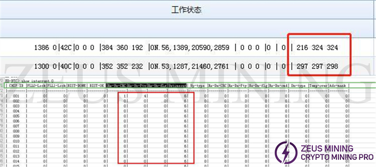
Repair methods for this failure:
① For boards with pull-down capacitors such as EBAZ789x, the C27 capacitor can be changed from 10pF to 20pF; for boards without pull-down resistors such as EBAZ7836, a 20pF capacitor can be connected in parallel with RB15;
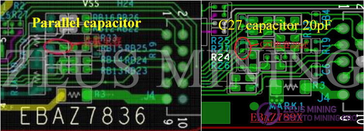
② If the first step cannot solve the problem, you can also add an external adapter board for maintenance;
③ If there is a small amount of errors at power-on, it does not need to be repaired without increasing the error and not affecting the hash rate.
(2) The number of single chip errors is concentrated and relatively large:

① If the hash board sometimes shows high temperature temp-over, first check whether the silicone grease is brushed well, if there is any abnormality, you need to brush the silicone grease again;
② If the temperature is too high and the brushing of silicone grease is ineffective, try to replace the ASIC chip;
③ If you find that the hashrate of the asic chip at the this level or at the same level is low or zero and the core voltage is high, just replace the ASIC chip;
④ If there are several consecutive levels of xx_DN_xx errors, check whether the chip at the front level is well soldered or whether there is tin connection;
⑤ Follow-up will communicate with the software, and directly display the single chip with a large number of errors, so as to facilitate the positioning of specific chip repairs;
VII. Partial schematic and PCB sharing
1. Schematic (MCU) part
(1) The AD part is leakage detection;

(2) EERPOM is the version number displayed by the gadget. The wrong version number means that there is a problem with this circuit (excluding communication abnormalities). This circuit failure generally does not affect the running hash rate;

(3) If the indicator light is off or always on, first check whether the input powering LDO-3.3V is normal;
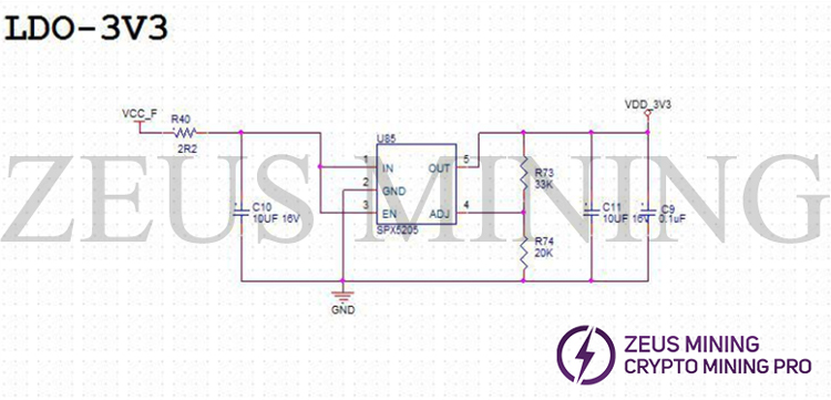
(4) OSC is the crystal oscillator on the hash board, which is used for the XCLK clock signal of the asic chip.
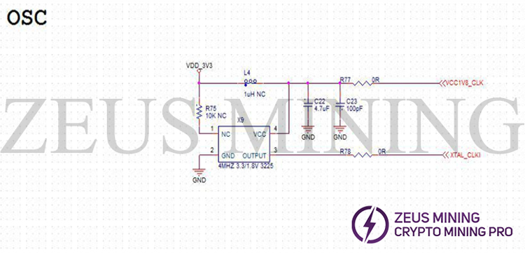
(5) Boost circuit, which provides power supply to the periphery of the chip. Usually, if this circuit fails, there has no hashrate, and the last 10 groups of ID scans are wrong. Usually replacing U80 and U87 can eliminate the fault, where U80 outputs the last 1, 3, 5, 7, 9 groups, and U87 outputs the last 2, 4, 6, 8, 10 groups. If it cannot be ruled out, there is a short circuit in the asic chip. This circuit needs to be ruled out before it can be repaired.
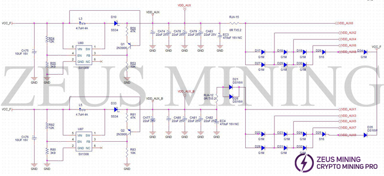
2. PCB boost circuit part

3. Principle signal part
The voltage of the data part will change when running the test program, the clock is usually fixed at an intermediate value, and other signals are high level or low level.
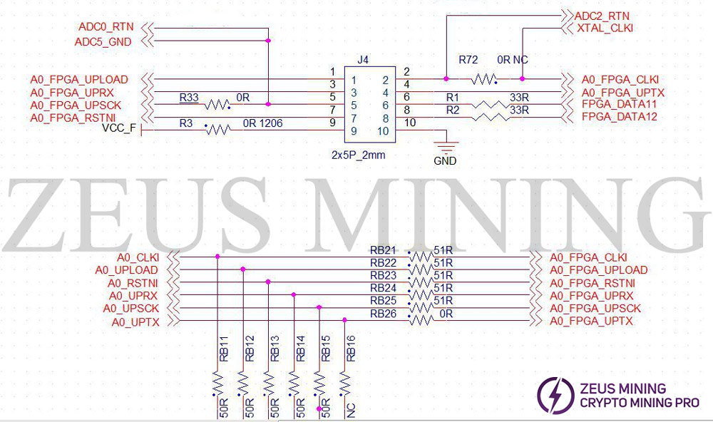
(1) PCB signal part
The PCB signal cable needs to check whether there is an open circuit (the upper row of resistors is usually 33~75 Ω), if the resistor is open and short circuited, the corresponding group may not be able to obtain the ID.

(2) The chip cascading part of the schematic diagram
The chip mainly checks the voltage between VDD_HK---VSS, usually not lower than 0.25V~0.5V, normal, too low may short circuit, LDO failure; too high may open circuit.
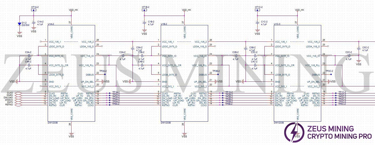
(3) PCB chip cascading part
Each stage has 3 ASIC chips (powering unit is in parallel, signals are in serial).

We use cookles to Improve your online experience. By continuing browsing this website, we assume you agree our use of cookies.