


During the production and use of the miner, if the user encounters a chain failure, low hash rate, and many hardware errors, please refer to this manual for test repairs.
Note: This manual cannot cover all possible abnormal problems. If you encounter problems that cannot be repaired according to the manual, please check the official website Innosilicon troubleshooting page; we will update the latest content from time to time.
I. Overview
1. Hash board circuit layout and test point distribution
Take the Innosilicon A4+ hash board as an example; please refer to the relevant design documents for other models.

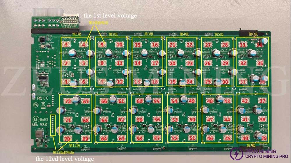
1) The six adjacent chips in the figure are a voltage domain [(1,2,3,4,5,6),...(67,68,69,70,71,72)], a total of 12 voltage domains, and the voltages of the six chips in each voltage domain are the same. The average voltage of each voltage domain at startup is about0.45V;
2) The blue arrows in the figure show the direction of CLK and communication signals;
3) There are 1-7 test points between every two chips. Test points 1 to 7 are CLK, RST, EN, SCK, CS, DI, and DO signals.
Specifically as shown below:

4) Test point and connection between front and back chips:

2. Test software instructions
Software | Use occasions | Illustrate |
Test chain | After SMT, stick before the heatsink. | Used to quickly check welding problems, not do long-term functional tests, only test all chips to communicate normally. |
Before sticking | After sticking the heat sink on the non-chip side. | It is used to check various defects of the single board in the high power state as soon as possible. With one less heat sink, the operating frequency of the chip is lower than that in normal use. |
Binning after sticking | After all the heat sinks are pasted. | Execute the test under 4 working voltages, and classify the board according to the measured hash rate files. The same gear single hash board is loaded into the same miner. |
Repair | Positioning the single hash board problem. | The program will send unlimited communication commands for maintenance personnel to use the multimeter, oscilloscope checks the necessary circuits. |
Aged | Miners are aged before leaving the factory. | Use official factory firmware. If there is any abnormality, an error code will be displayed on the mass production management interface. |
3. List of error codes for testing software before and after sticking
If there is no problem with the detection, "√" will be printed at the end of the log, otherwise, "×" will be printed. In the event that a problem is detected, the software will report the error type with the highest priority,and the error priority order is: E0 > E9 > E6 > E4 > E7 > E5 > E3 > E1 > E2 > E8. This report can guide the maintenance and replacement of chips.
Error code | Describe | Remark |
E0 | Chip Type is not found. | Chain failure. |
E1 | The number of good cores on a single chip is less than 30%. | Statistics under working frequency. |
E2 | The number of good scores on the whole board is less than 90%. | Statistics under working frequency. |
E3 | Single-chip job test is all wrong. | |
E4 | Chip PLL does not lock. | |
E5 | Abnormal chip temperature. | The software reports 9999 or -9999. |
E6 | Abnormal chip voltage. | |
E7 | The command returns an error, or the frequency increase fails. | "E7:0" means pll configuration failed. |
E8 | The total error rate of the whole board job test is greater than 10%. | |
E9 | The number of reading chips is incorrect. | |
E10 | (Reserved) | |
E11 | Can't find a suitable gear after sticking. | |
E12 | Command returns CRC error. | |
E13 | Buck failure. |
4. Aging software error code list
Serial number | Question | Solution | Notice |
1 | Control board IO failure | Replace the control board | Factory reset must be done when done |
2 | Control board network failure | ||
3 | Hash board failure | Replacing the hash board | After completion, you must restore the factory settings or re-aging. |
4 | Chip failure | ||
5 | Individual chip temperature is too high | ||
6 | Electricity failure | Replace the power supply | After completion, it is recommended to restore factory settings or re-aging. |
7 | Communication signal line interference | Use shielded wire | |
8 | The communication signal line is not plugged in properly | Check and re-plug the communication signal cable | |
9 | The power consumption of the whole miner is too high | Re-aging or downclocking (Efficiency mode) | |
10 | The ambient temperature is too high | Improve the operating environment | |
11 | Fan failure | Check the fan cable connection, check whether the fan model matches, and check whether the fan is installed in the correct direction | Refer to the document control board FAQ. |
12 | Mining pool setting error | Check pool settings or factory reset | |
13 | The network cable is not plugged in | Check the network cable connection | |
14 | Network environment failure | Check the switch configuration such as DHCP and DNS |
Err Code | Description | Err Message | Analysis |
0 | Normal | - | Normal |
21 | 1 or more hash boards not detected | The number of the detected hash board, if there is more than one separated by a space | Communication signal line is not plugged in / control board IO failure / hash board failure |
22 | Power communication error | - | Power failure / control board IO failure |
23 | All hash board encore failed | - | Control board IO failure / power failure / hash board failure |
24 | Part of the hash board encore failed | encore The normal hash board number, if there are multiple numbers separated by spaces | Hash board failure / control board IO failure / power failure |
25 | Upscaling failed | Hash board number: Error frequency point | Communication signal line interference / hash board failure |
26 | Failed to set voltage | Hash board number: 1/2 | Communication signal line interference / hash board failure |
27 | Bist failed | Hash board number: 1/2 | Communication signal line interference / hash board failure |
28 | Runtime communication signal Error cannot be recovered automatically | Hash board number | Communication signal line interference / hash board failure/control board IO failure |
29 | I2C communication failure at runtime cannot be automatically recovered | - | Power failure/control board IO failure |
30 | Can't connect to a mining pool | - | Mining pool setting error / network cable not plugged in / control board network failure / network environment failure |
31 | Damage to individual chips, leading to inflated hash rates | Damaged chip number: hash board number; if there is more than one, separate them with spaces | Chip failure |
32 | Over-temperature | Hash board number | Ambient temperature is too high / fan failure / individual chip temperature is too high / power consumption of the whole miner is too high |
33 | Failed to read the temperature | Hash board number | Control board IO failure/hash board failure |
34 | Communication signal cable connection is abnormal | Hash board number | The communication signal port of the control board is inserted incorrectly/the IO of the control board is faulty |
35 | Insufficient power supply | Hash board number: chip number | PSU failure |
36 | The number of good cores in the chip is abnormal | vidtype, minertype, subtype, chipnum | Hash board failure |
37 | The wrong type of control board vid | - | Hash board failure |
II. Maintenance preparation
Tools: serial board, data cable, TF card, jumper cap, oscilloscope, multimeter.
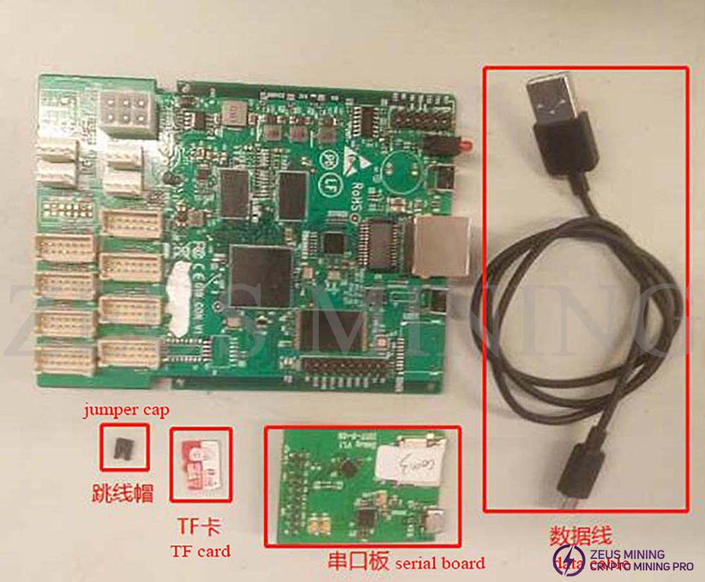
Required software: boot.bin, SecureCRT.exe.
1. Maintenance software instructions
1) How to use boot.bin
How to use: After shutting down, copy xxx.bin directly to the TF card, insert the TF card into the slot of the serial board, connect the serial board to the control board, and use the jumper cap to connect to the J2 interface, then power on.
2) Serial port tool description
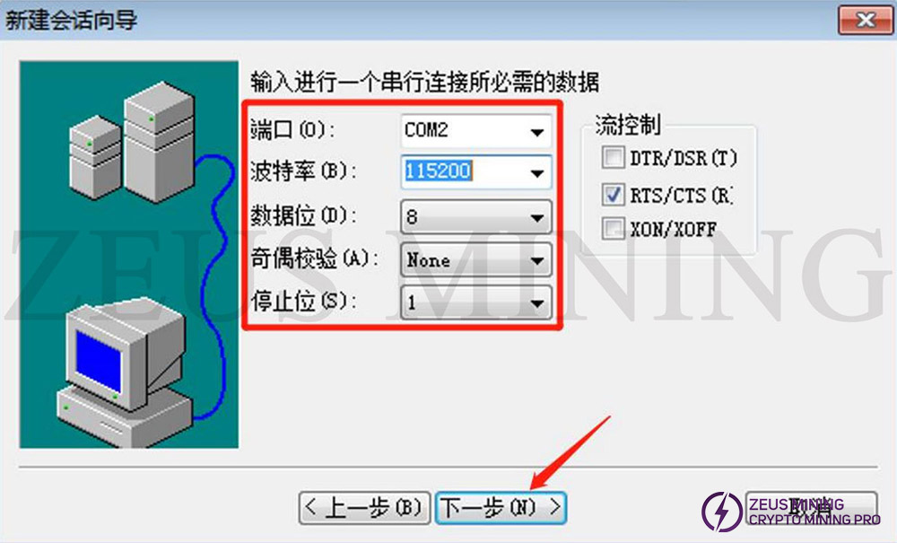
Install the serial port test tool on the computer, and set the baud rate: 115200, n, 8, 1.
The setting method is as follows:
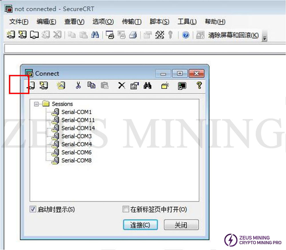
a. Double - click the serial port icon to open the serial port tool as shown in the figure below, and click "New Dialog" in the red dialog box.
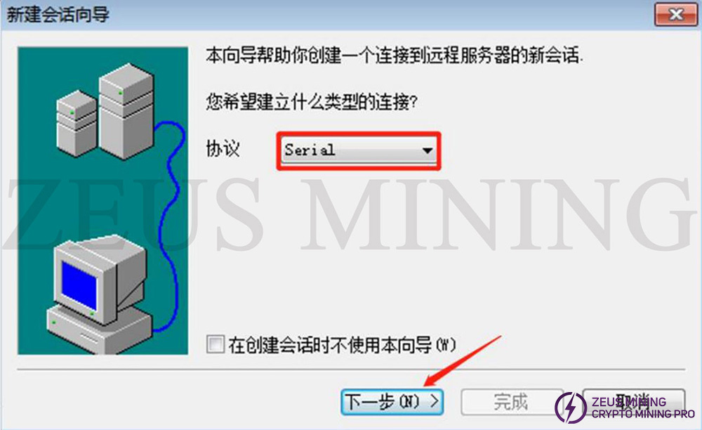
b. Select the serial port protocol in the new session wizard.
c. Set the baud rate: 115200 and other options.
3) Instructions for the use of normal software
Software before and after sticking
The Normal software usage process is as follows:
a. After inserting the SD card into the slot, check that the device is correct, and then power on.
b. Open the serial port software to check whether the software version information is correct after power-on.
c. During the testing process, test information is displayed and prompts characters at various stages to facilitate hardware testing and status monitoring.
d. After the end of the test, print the test results. If it is a multi-chain test, the test results will be printed together after the end.
e. Re-test, press the Reset button directly on the control panel or press the Enter key according to the prompt software character.
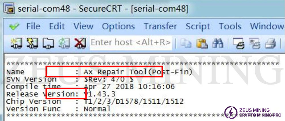

Repair software
a. After inserting the SD card into the slot, check that the device is correct, and then power on.
b. Open the serial port software to check whether the software version information is correct after power-on.
c. During the test, there will be a test information display and LED light display at various stages to facilitate hardware testing and status monitoring.
d. The software will continuously send a certain fixed command moment during the running process, which can be used to measure voltage and signal.
e. After the measurement is completed, press the function key to continue running backward and print the test results.
f. Re-test, press the reset key directly on the control board or press the Enter key according to the prompt software character.
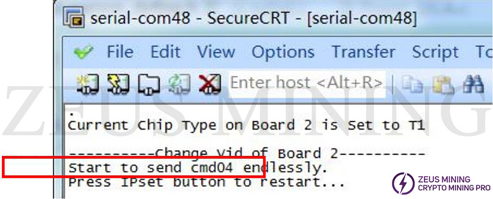
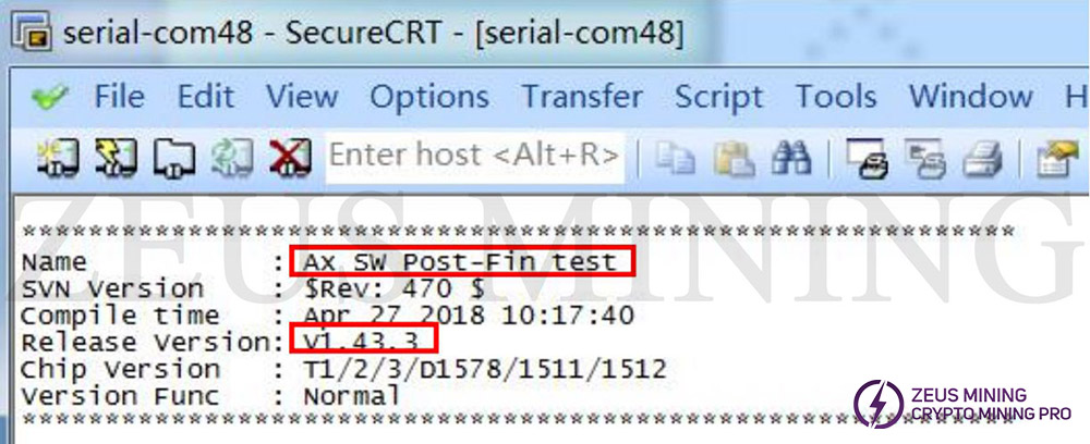
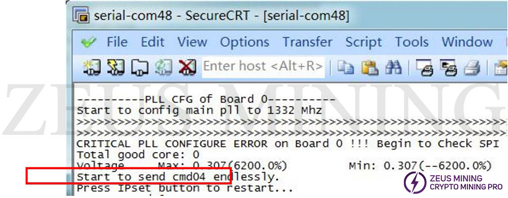
It should be noted that the maintenance software can only test one circuit board at a time. Only the corresponding indicator light is off when the function key is pressed to ensure that the key is successfully captured.
2. Test environment setup
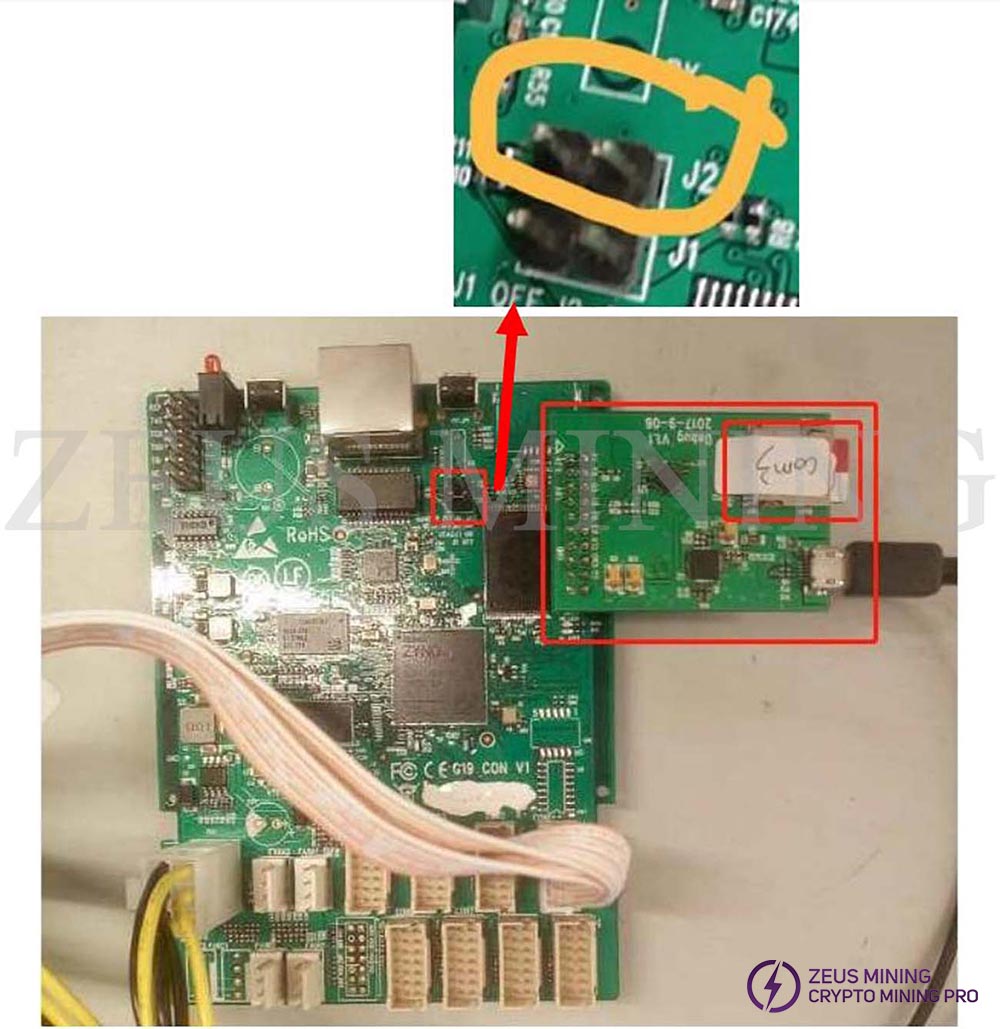
Take out the miner control board to be tested, insert the TF card into the control board and serial port board according to the position shown in the figure, and insert the jumper cap into the interface shown in the figure. Connect the serial board and the computer with a data cable.
III. Maintenance process
1. The basic process of the whole miner's aging and poor maintenance
1) To reproduce the problem of poor aging, record the error code.
2) Check whether the power output corresponding to the defective board is normal.
3) If it is a power supply controlled by multiple channels, swap the wrong board and the normal board for the power channel (note that the order of the data cable interface is adjusted at the same time), and observe whether the phenomenon follows the hash board or the power supply. If it follows the power supply, replace it and redo the aging.
4) Disconnect the power supply and network cable. Check the miner for damage to the exterior. Check whether the power and data cable connections are loose or disconnected.
5) Use the original miner power supply and the faulty hash board, do the post-stick test in the bucket, and record the error code and log.
6) Use the original miner power supply and the faulty hash board to test after sticking outside the barrel to see if the phenomenon still exists and make a record. If the chip surface is a heat sink fixed with screws, remove the heat sink on the chip surface and run a test to see if the phenomenon still exists and make a record.
7) Continue to analyze the defective repair process of the single hash board.
2. The basic process of single-hash board defective repair
Before maintenance, please confirm that the power supply, control board, and various cables are correctly connected.
1) Use the pre-stick test software to test and get the error code Ex:x. Different next steps may be taken for different types of errors.
2) Check the appearance of the hash board to see if there are missing components, errors, or abnormal appearances. For example, check whether there are solder balls, foreign objects, etc., near the error chip.
3) Run the maintenance procedure and check the input voltage with a fluke 15B+ multimeter. Check the crystal oscillator power supply. Check the tail IO boost circuit. Finally, check all levels of LDO output.
4) Use an oscilloscope to check the chip input and output signals CLK, SCK, DO, DI, CS, RSTN, and START.
5) If it is found that the output signal of the hash board chip is abnormal, do not replace it easily. First, try adding soldering, re-soldering, and swapping with other chips on this hash board.
6) If the chip swap method is used, it can be observed whether the problem follows the chip.
7) After the above methods are invalid, replace the chip.
3. The special maintenance program locates the broken chain position
Copy the provided repair.bin into the TF card and insert it into the serial board. Connect the power supply and data cable (no fan is required), and power on. Cooperate with the software error message before or after sticking, and measure the test of the relevant chip and its adjacent chips point.
Description of the function keys and indicator lights in the maintenance software.
1) The light on the power-on control board is on (red and green lights beside the reset button); if the power-on chain is broken, cmd04 will be sent all the time; after pressing the function key next to the USB card slot, stop sending cmd04, and the program will continue to execute, this When the green light is off;
2) If the power-on chain is connected, it will continue to send cmd04. After the same function key is pressed, it will stop sending cmd04, and the green light will be off;
3) After the frequency configuration fails, cmd04 will be sent at the point of failure. After pressing the function key, the sending of cmd04 will stop, the program will continue to execute, and the red light will be off at this time;
4) After the frequency configuration is successful, if the chain is broken during the continuous reading of the chain, cmd04 will be sent to the broken chain. After pressing the function key, it will stop sending, and the red light will be off simultaneously, and the program will continue to execute.
IV. Analysis of typical problems
1. E0: 1
This type of problem is that the communication chain is completely blocked, and most of them are caused by abnormal peripheral circuits. Known causes are:
1) The power supply has no output or abnormal output.
2) The tin is short-circuited between the pins of the communication interface connector.
3) The data cable is not plugged in properly, has poor contact, or is damaged and short-circuited.
4) The device between the communication interface and the first chip is defective, such as false welding, short circuit, burning, displacement, missing parts, etc.
5) The first chip IO was damaged by static electricity.
6) The crystal oscillator is abnormal.
7) Parts are missing.
If you encounter such problems, you need to complete the inspection according to the "V Checklist".
2. E0: N
The problem is that the communication chain is partially blocked, and it is broken at the Nth chip. Known causes are:
1) The signal between the Nth and N-1th hash board chips is abnormal, and the related pins of the two chips are falsely welded, floated high, short-circuited, and IO damaged.
2) The peripheral devices of the Nth chip are falsely welded, short-circuited, burned, displaced, missing parts, etc.
Repair steps:
a. Check the peripheral circuit; if there is no abnormality, go to the next step.
b. Check N and the IO pin-to-ground resistance of each hash board chip in the front and rear. If there is no abnormality, go to the next step. If there is any abnormality, remove the chip and compare the IO-to-ground resistance of the new chip. Again, if there is no apparent difference, go to the next step. Otherwise, replace the chip.
c. Resolder N and N-1 chips, go to the next step if there is still abnormality.
d. In other cases, it is necessary to use maintenance-specific programs to assist positioning. For example, it is measured when the software executes "Start to send cmd04 endlessly". It is necessary to measure the abnormal chip voltage with a Fluke 17B+ multimeter and measure the Nth and N-1th chip signals with an oscilloscope. If the output DO/CS/SCK of the N-1th chip is abnormal (it can be compared with the normal waveform of the chip before the N-1th, if the waveform is inconsistent, it is abnormal), then replace the N-1th chip; if the Nth chip output is abnormal, then replace the Nth chip. If the output of the Nth chip is normal, but the input DI is abnormal, then replace the N+1th chip.
3. E6: N
The voltage of the Nth chip is abnormal. Maintenance method:
1) Use a multimeter to confirm whether the chip's voltage is abnormal. If the chip's voltage is too low, measure the SCK signal at the test points of the three chips at this level, and compare the chip whose SCK frequency is jittered with other chips of different levels with higher partial voltages swap. If the SCK is normal, replace chip N with other chips of different levels with higher partial pressure.
2) If the problem follows a chip, replace the chip.
4. E7: 0
When E7:0 occurs, you need to locate the problem through the maintenance software. The positioning method is the same as E0. The test time is when the program runs to "CRITICAL PLL CONFIGURE ERROR on Board 0 !!! Begin to Check ..."
5. E7: N
Indicates that the chip N has no return, replace the chip. The checking method is the same as E0:N.
6. E1: N
The Nth chip has fewer cores. If this problem occurs in a large area, it is recommended to report it to our technical staff. If very few hash boards have this problem, replace chip N.
7. E2
There are few total cores on the hash board. First, check whether the total voltage of the circuit board is abnormal (refer to the method in E0 error). If there is no abnormality, you need to send it to the nearest repair center.
8. E3: N
The Nth chip has a high softbist error rate. The processing method is the same as E1: N.
9. E4: N
The Nth chip pll is not locked. Check N-1 chip output CLK if there is no abnormality, resolder N-1 and N chips. If it still can't be solved, replace the N chip.
10. E5: N
If the temperature of the Nth chip exceeds the standard, replace the chip. If the problem occurs in a large area, check the heat sink, and if it still cannot be solved, you need to send it to the nearest repair center for repair.
11. E8
The whole hash board softbist has a high error rate. It detects whether the circuit board voltage and the CLK of each chip are abnormal. If it is abnormal, replace the abnormal chip. If there is no abnormality, it needs to be sent to the nearest repair center for repair.
V. Checklist
This checklist is for maintenance reference.
Check items | Result |
1. Process inspection | |
Check Point 1. Whether the solder joints of the chip are full and whether there are tin beads. | |
Check Point 2. Are there any components falling off? | |
Check Point 3. Whether the silicon grease or thermal pad covers the chip. | |
2. Check the error message of the test software before or after sticking | |
Check Point 4. Correct identification of chip type. | |
Check Point 5. The reading status is normal at the default frequency (all chips' Frequency=60Mhz, Main PLL Lock=1, Temperature, Voltage within reason). | |
Check Point 6. Successfully ramped up to the operating frequency (PLL frequency.) | |
Check Point 7. The reading status is normal at the working frequency (all chips' Frequency=working frequency/2, Main PLL Lock=1, Temperature, Voltage within reason.) | |
Check Point 8. Soft Bist of Error rate within a reasonable range (less than10%.) | |
Check Point 9. Test software result is tick. | |
3. Power Output | |
Check Point 10. There is no abnormality in the voltage output from the power supply to the hash board (refer to the specifications of the specific model.) | |
Check Point 11. Power output control board voltage12V±10%. | |
4. Control signal (measured after the hash board is powered on) | |
Check Point 12. EN_CORE=3.3V±10% | |
Check Point 13. RESET=1.8V±10% | |
Check Point 14. START=1.8V±10% | |
5. Hash board chip voltage | |
Check Point 15. Total CORE voltage should be consistent with the output voltage of the power supply. If the VID settings are unreasonable or the settings do not take effect, it will cause abnormal or unstable work. If the VID setting does not take effect, check whether the software and hardware programs of the control board are correct. | |
Check Point 16. All levels of IO voltage should always remain1.8V. All levels of IO voltage should always remain1.8Vleft and right; in exceptional circumstances, IO voltage may be lower than1.6V. IO pin aging or damage, which may cause IO abnormal voltage. | |
Checkpoint 17. All levels when starting and increasing the frequency Core voltage greater than 0.32V, less than 0.6V. At the default frequency, all CORE voltage levels may vary greatly, and the reasonable value is 0.32V to 0.6V. | |
6. Clock signal quality | |
Check Point 18. The clock output from the crystal oscillator to the first chip is12Mhz±1%, duty cycle 50%, no obvious shaking move, amplitude 1.8V±10%. | |
Check Point 19. The last chip outputs the clock is 12Mhz±3%, the duty cycle is at 30%~70% between, no display jitter, amplitude1.8V±10%. | |
Check Point 20. The input clock of the chip at all levels in the middle is 12Mhz±3%, the duty cycle is at 30%~70% between, no display jitter, amplitude1.8V±10%. | |
7. Measure and analyze the test points before and after the first chip where the communication signal chain is broken(denoted as TN.) | |
Check Point 21. Check whether the error-reported chip and the pin-to-ground resistance of the front and rear chips are abnormal. Compared with other normal chips. | |
Check Point 22. The CLK of TN-1 and TN are both 12Mhz, and there is no apparent jitter, the duty cycle is basically1:1. | |
Check Point 23. When the maintenance program sends commands, the communication signals of TN-1 and TN test points are not abnormal. It can be compared with the normal waveforms of chips before N-1; it is abnormal if the waveforms are inconsistent. |