


How to convert the Ebit E9+ control board into the Zynq development board? The article explains this in detail.
Chapter 1: Change the SD card to start and change the power supply
1. The positive and negative electrode of the power interface is shown in the figure below. When connected, pay attention not to be reversed.

2. If you use the J4's 6P power interface, you need to short-circuit the D24 on the back or weld a diode, as shown below:
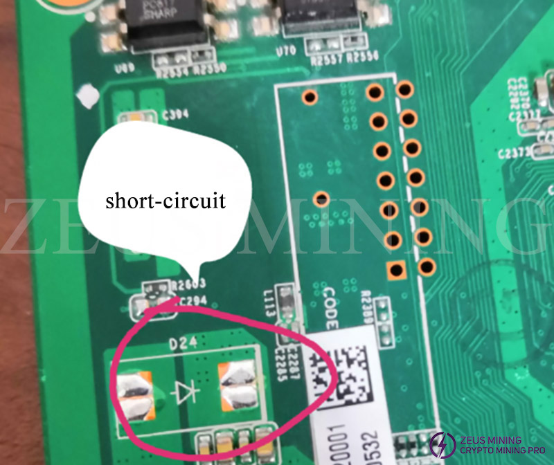
If there is no diode, you can move D21, D22 and D23, and pay attention to the polarity of the diode.
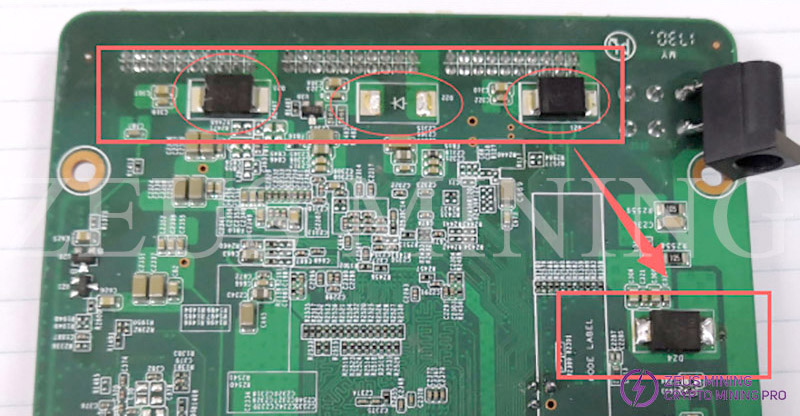
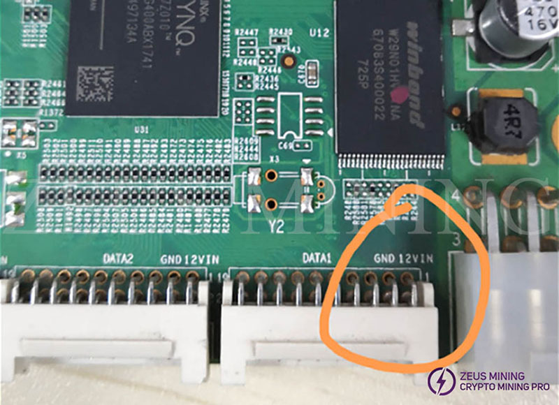
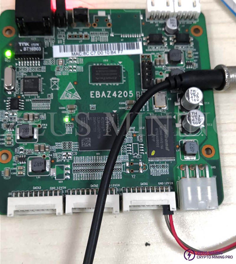
If there is no 6P power supply, you can also weld the power unit of a DC-005; as shown in the figure above, pay attention to the direction. You can also connect the PIN 1 (12V) Pin 3 (GND) of the PHD2.0 interface Data1, Data2, and Data3, as shown below:
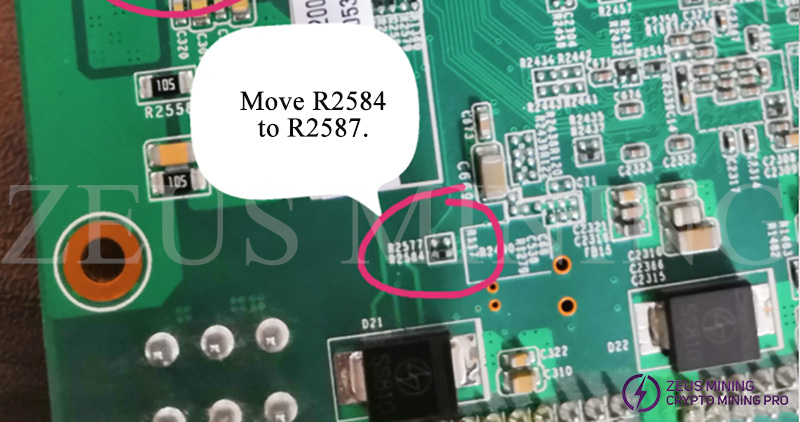
3. The easiest way to change the SD card is to short-circuit the R2577 or move the R2584 to the R2577, and change it to NAND to start and change it back. As shown below:
1) serial position J7, welding TX, RX, GND, the baud rate is 115200. SD card is just welded directly.
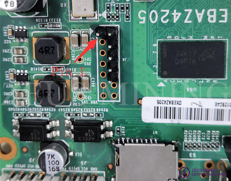
2) JTAG port is J8, and the pin that needs to be used is:
PIN1 (GND), PIN2 (VREF), PIN4 (TMS), PIN6 (TCK), PIN8 (TDO), PIN10 (TDI).
After changing the SD card, put the ![]() on the SD card, and you can start with the SD card. It was found that the green and red lights flashed every second.
on the SD card, and you can start with the SD card. It was found that the green and red lights flashed every second.
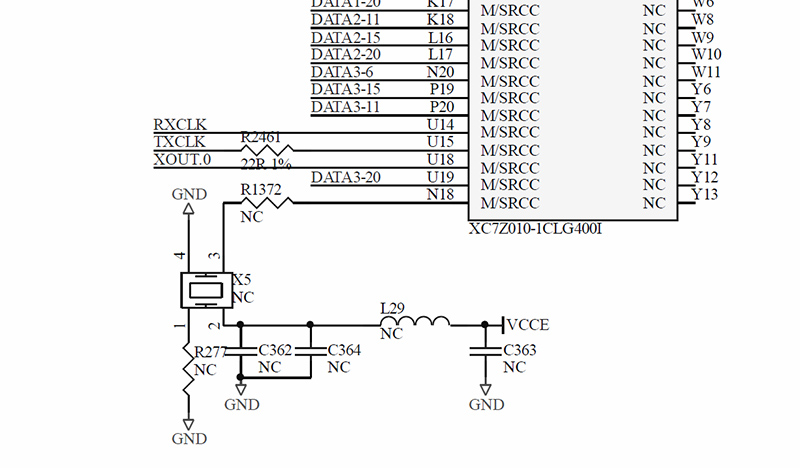
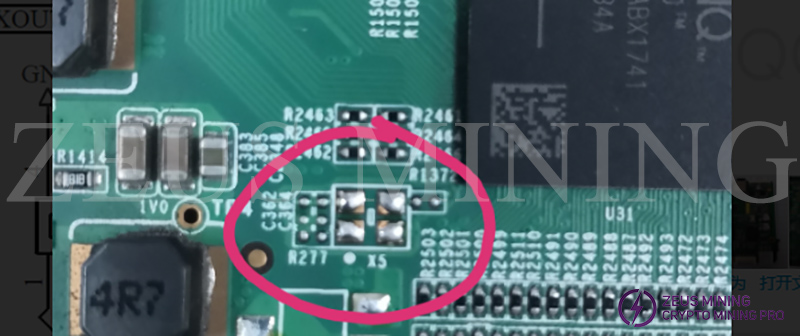
3) If the crystal on the PL terminal is needed, the circuit diagram is as follows: the R1372 welded with a resistor below 50 ohms. L29 can be directly short-circuited; as for the crystal's size, welding a crystal source with 3225 packaging below 50MHz according to its needs. There is PLL inside FPGA to double frequency.
The position of the crystal on the board is shown below.
Chapter 2: Establishment of engineering file
Zynq settings are as follows: (Example engineering version files are vivado 2018.2; other versions are almost the same.
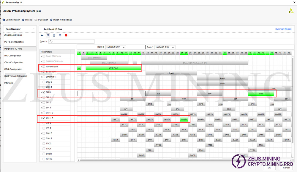
As shown in the figure above, the selection of NAND Flash, SD cards, and UART1 is as above, and the green indicates that it has been selected.
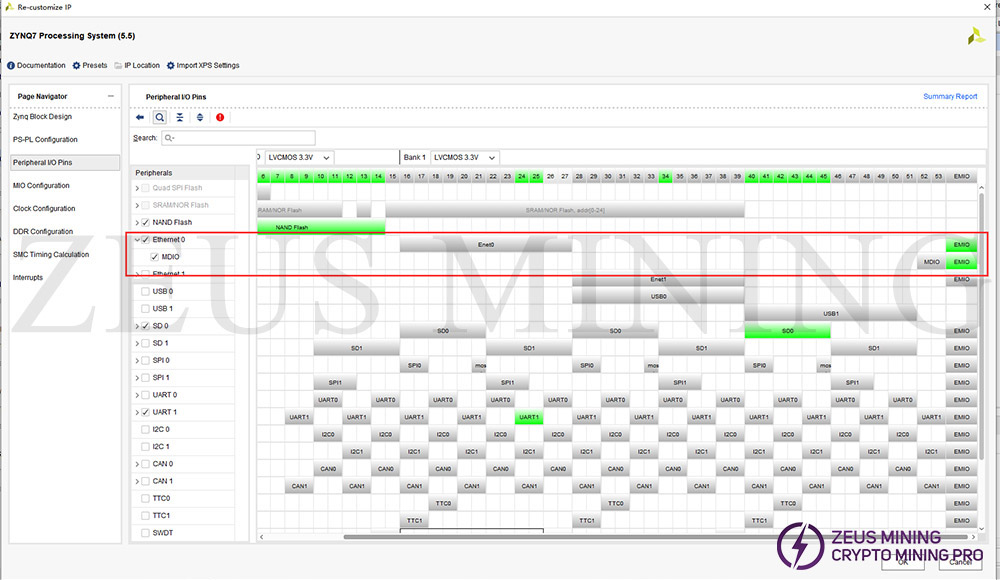
As shown in the figure above, the mesh is checked MDIO, and all choose EMIO. For tube feet, please refer to the top.xdc file in the project.
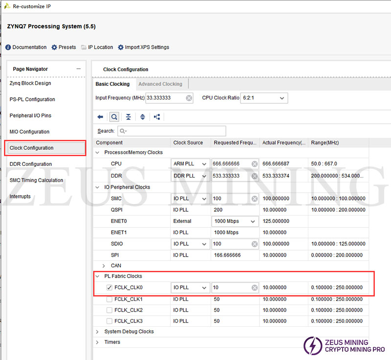
As shown in the figure above, because the crystal vibration of the FPGA side is selected, the clock used by the FPGA is led from the PS side. Therefore, you need to select FCLK_CLK0, and the output clock frequency can be set by yourself.
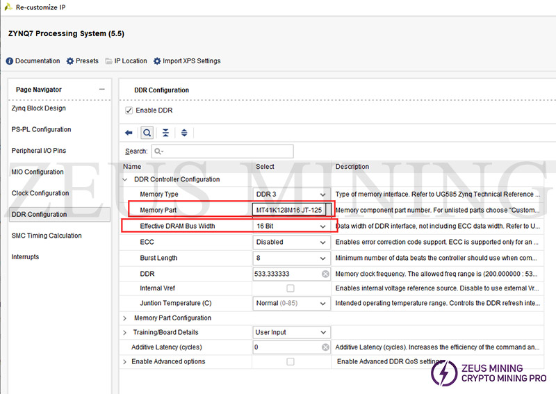
As shown in the figure above, the setting of DDR, MEMORY PART chooses MT41K128M16JT-125, and the data bits are selected as 16bit.
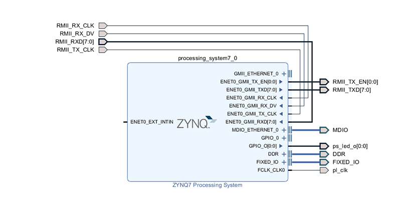
As shown in the figure above, the drawing diagram of each pin should pay special attention to the RMII interface.